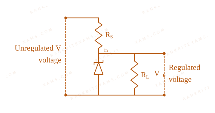
The following diagram shows a Zener diode as a voltage regulator. The Zener diode is rated at V_Z = 5V$V_{Z} = 5V$ and the desired current in load is 5 mA. The unregulated voltage source can supply up to 25V. Considering the Zener diode can withstand four times of the load current, the value of resistor R_S$R_{S}$ (shown in circuit) should be ____ Omega$\Omega$.
Circuit containing unregulated voltage, series resistor Rs, Zener diode, and load resistor.
A.4000$4000$
B.10$10$
C.100$100$
D.1000$1000$
Solution & Explanation
### Related Formula
I_texttotal = I_Z + I_L$$I_{\text{total}} = I_{Z} + I_{L}$$V_textin - V_Z = I_texttotal R_S$$V_{\text{in}} - V_{Z} = I_{\text{total}} R_{S}$$
### Core Logic
The question is dropped by the examination authority, meaning there was an anomaly in data or multiple correct interpretations, likely due to imprecise wording regarding the maximum source voltage and the exact safe current rating. In a nominal calculation, I_Z_textmax = 4 times 5 text mA = 20 text mA$I_{Z_{\text{max}}} = 4 \times 5 \text{ mA} = 20 \text{ mA}$. Total current I = 25 text mA$I = 25 \text{ mA}$. R_S = (25 - 5) / (25 times 10^-3) = 800Omega$R_{S} = (25 - 5) / (25 \times 10^{-3}) = 800\Omega$, which is not in the options.
### Step 1: Final Conclusion
Question Dropped.
### Pattern Recognition
Sees: "Question Dropped" → This often occurs when mathematical data maps to none of the provided MCQs.
### Evaluation Rubric / Model Answer
null
### Chapter Mix
Class 12 Physics: Semiconductor Electronics: Materials, Devices and Simple Circuits
Keywords:#Zener diode voltage regulator#JEE Main 2026 Morning Q37#Semiconductor Electronics: Materials, Devices and Simple Circuits JEE Main 2026#Zener Diode JEE Main 2026#Zener regulator#voltage source#series resistor#load resistor
More Semiconductor Electronics: Materials, Devices and Simple Circuits Previous-Year Questions
Qjee_main_2026_21_jan_morningLogic Gates
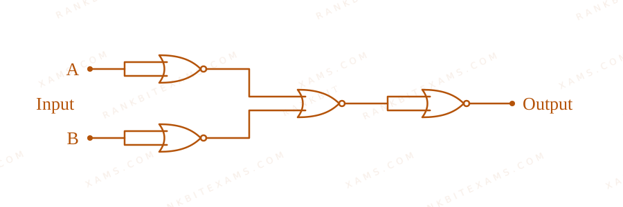
The given circuit works as :
Circuit containing multiple interconnected logic gates leading to a final output.
A. AND gate
B. NOR gate
C. NAND gate
D. OR gate
Solution
### Related Formula
De Morgan's Laws:
overlineA + overlineB = overlineA cdot B$$\overline{A} + \overline{B} = \overline{A \cdot B}$$overlineoverlineA = A$$\overline{\overline{A}} = A$$
### Core Logic
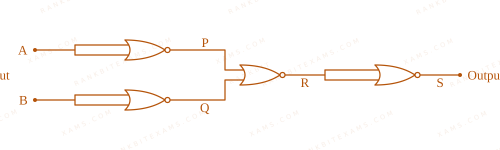
Analyzing the circuit diagram:
Circuit containing multiple interconnected logic gates leading to a final output.
- Top branch has a NOT gate on A, so P = overlineA$P = \overline{A}$
- Bottom branch has a NOT gate on B, so Q = overlineB$Q = \overline{B}$
- They enter a NOR gate, giving output R = overlineoverlineA + overlineB$R = \overline{\overline{A} + \overline{B}}$
- Finally, R passes through a NOT gate to give S = overlineR$S = \overline{R}$
### Step 1: Boolean Simplification
R = overlineoverlineA + overlineB = overlineoverlineAB = AB$$R = \overline{\overline{A} + \overline{B}} = \overline{\overline{AB}} = AB$$S = overlineR = overlineAB$$S = \overline{R} = \overline{AB}$$
The expression overlineAB$\overline{AB}$ is the Boolean expression for a NAND gate.
### Pattern Recognition
Two NOTs feeding into a NOR equals an AND gate (AB$AB$). Adding a final NOT gate turns the AND into a NAND.
### Evaluation Rubric / Model Answer
null
### Chapter Mix
Class 12 Physics: Semiconductor Electronics
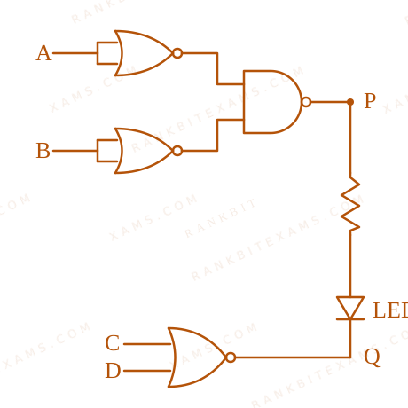
### Related Formula
textNOR Gate: overlineA+B, quad textNAND Gate: overlineA cdot B$$\text{NOR Gate: } \overline{A+B}, \quad \text{NAND Gate: } \overline{A \cdot B}$$
### Core Logic
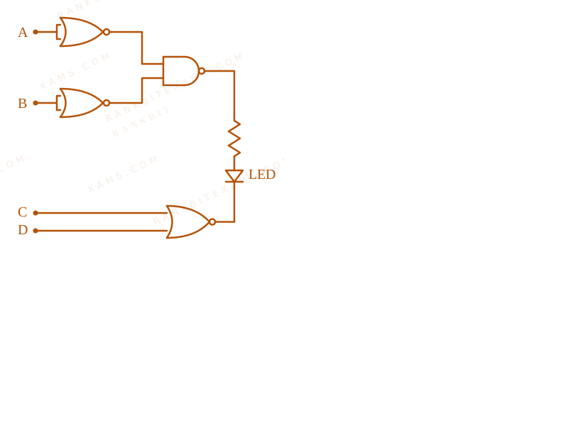
Logic gate circuit diagram connected to an LED.
LED will glow in forward biasing when point P is at higher potential (1) and point Q is at lower potential (0).
Testing option (4) [1101]:
- Inputs A=1, B=1 through NOR and NAND gates yield P = 1.
- Inputs C=1, D=0 through NOR gate yields Q = 0.
- Forward bias established, LED glows.
### Pattern Recognition
Sees: Logic gates combination with LED forward biasing condition.
Shortcut: Check forward bias requirement (P=1, Q=0) for each option combination.
Check: Option (4) satisfies the condition. ✓
### Chapter Mix
Class 12 Physics: Semiconductor Electronics
Q35jee_main_2026_22_january_eveningLogic Gates and Truth Tables
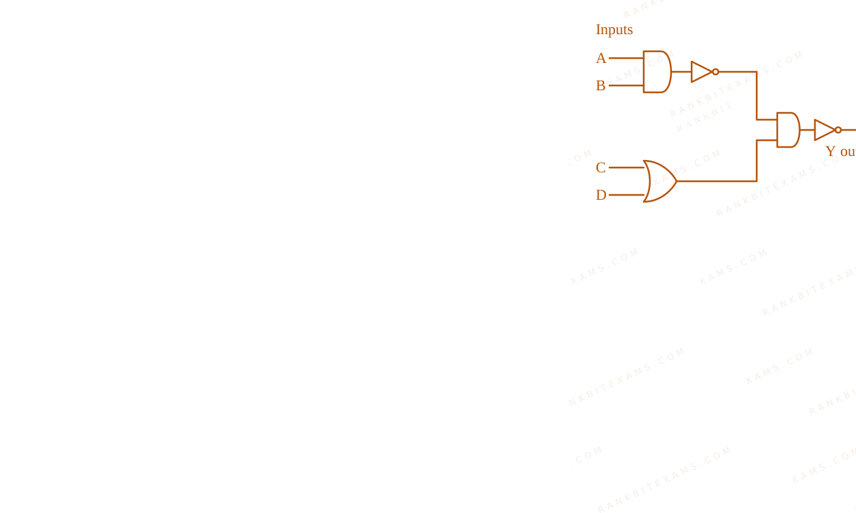
The correct truth table for the given input data of the following logic gate is :
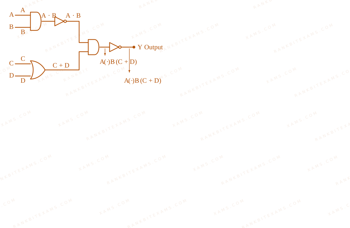
The figure illustrates a combined logic circuit with inputs A, B, C, D feeding into AND, OR, and NOT gates to produce output Y.
A.
Inputs
Output
A
B
C
D
Y
1
1
0
1
1
0
0
1
1
0
1
0
1
0
1
1
1
1
1
0
B.
Inputs
Output
A
B
C
D
Y
1
1
0
1
1
0
0
1
1
0
1
0
1
0
0
1
1
1
1
1
C.
Inputs
Output
A
B
C
D
Y
1
1
0
1
0
0
0
1
1
0
1
0
1
0
1
1
1
1
1
1
D.
Inputs
Output
A
B
C
D
Y
1
1
0
1
0
0
0
1
1
1
1
0
1
0
1
1
1
1
1
1
Solution
### Related Formula
Y = overline(overlineA cdot B) cdot (C + D)$$Y = \overline{(\overline{A \cdot B}) \cdot (C + D)}$$
Applying De Morgan's Law:
Y = (A cdot B) + (overlineC + D)$$Y = (A \cdot B) + (\overline{C + D})$$
### Core Logic
Analyzing the expression step by step:
1. Upper branch: A$A$ and B$B$ pass through NAND gate rightarrow overlineA cdot B$\rightarrow \overline{A \cdot B}$.
2. Lower branch: C$C$ and D$D$ pass through OR gate rightarrow (C + D)$\rightarrow (C + D)$.
3. Combined in AND gate followed by NOT gate (NAND equivalent output stage):
Y = overline(overlineA cdot B) cdot (C + D) = (A cdot B) + (overlineC + D)$$Y = \overline{(\overline{A \cdot B}) \cdot (C + D)} = (A \cdot B) + (\overline{C + D})$$
Testing conditions for Option (2):
- For A=1, B=1, C=0, D=1 implies (1 cdot 1) + (overline0 + 1) = 1 + 0 = 1$A=1, B=1, C=0, D=1 \implies (1 \cdot 1) + (\overline{0 + 1}) = 1 + 0 = 1$.
- For A=0, B=0, C=1, D=1 implies (0 cdot 0) + (overline1 + 1) = 0 + 0 = 0$A=0, B=0, C=1, D=1 \implies (0 \cdot 0) + (\overline{1 + 1}) = 0 + 0 = 0$.
- For A=1, B=0, C=1, D=0 implies (1 cdot 0) + (overline1 + 0) = 0 + 0 = 0$A=1, B=0, C=1, D=0 \implies (1 \cdot 0) + (\overline{1 + 0}) = 0 + 0 = 0$.
- For A=1, B=1, C=1, D=1 implies (1 cdot 1) + (overline1 + 1) = 1 + 0 = 1$A=1, B=1, C=1, D=1 \implies (1 \cdot 1) + (\overline{1 + 1}) = 1 + 0 = 1$.
The figure illustrates a combined logic circuit with inputs A, B, C, D feeding into AND, OR, and NOT gates to produce output Y.
### Step 1: Final Conclusion
Option (2) presents the correct truth table matching the evaluated output values.
### Pattern Recognition
Boolean reduction: overlinebarX cdot Y = X + barY$\overline{\bar{X} \cdot Y} = X + \bar{Y}$ where X = A cdot B$X = A \cdot B$ and Y = C+D$Y = C+D$. Hence Y = (A cdot B) + (overlineC+D)$Y = (A \cdot B) + (\overline{C+D})$.
### Evaluation Rubric / Model Answer
null
### Chapter Mix
Class 12 Physics: Semiconductor Electronics
Q38jee_main_2026_23_january_eveningLogic Gates
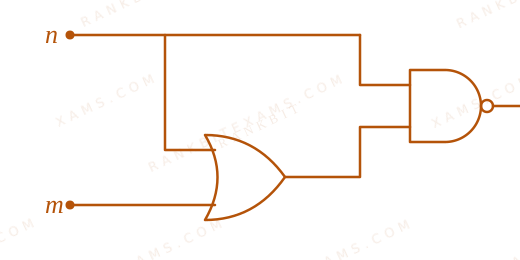
For the given logic gate circuit, which of the following is the correct truth table?
Circuit schematic containing an OR gate and a NAND gate.
A.
n
m
z
0
0
1
0
1
0
1
1
0
1
0
0
B.
n
m
z
0
0
0
0
1
1
1
1
0
1
0
1
C.
n
m
z
0
0
1
0
1
0
1
1
1
1
0
0
D.
n
m
z
0
0
1
0
1
1
1
1
0
1
0
0
Solution
### Related Formula
Boolean Algebra rules:
A + AB = A$A + AB = A$A cdot A = A$A \cdot A = A$
NAND Gate: Z = overlineX cdot Y$Z = \overline{X \cdot Y}$
### Core Logic
Gate 1 (Bottom): This is an OR gate with inputs n$n$ and m$m$.
Output = n + m$n + m$
Gate 2 (Top): This is a NAND gate. Its inputs are direct n$n$ and the output of the OR gate (n + m$n + m$).
Output z = overlinen cdot (n + m)$z = \overline{n \cdot (n + m)}$
### Step 1: Simplify the Boolean Expression
First, expand the inner term:
n cdot (n + m) = (n cdot n) + (n cdot m)$$n \cdot (n + m) = (n \cdot n) + (n \cdot m)$$
Since n cdot n = n$n \cdot n = n$, this becomes:
n + n cdot m = n(1 + m) = n cdot 1 = n$$n + n \cdot m = n(1 + m) = n \cdot 1 = n$$
So the overall output is:
z = overlinen cdot (n + m) = overlinen$$z = \overline{n \cdot (n + m)} = \overline{n}$$
### Step 2: Construct the Truth Table
Since z = overlinen$z = \overline{n}$, the output z$z$ only depends on n$n$ and is its exact inverse.
When n=0, m=0 implies z=1$n=0, m=0 \implies z=1$
When n=0, m=1 implies z=1$n=0, m=1 \implies z=1$
When n=1, m=1 implies z=0$n=1, m=1 \implies z=0$
When n=1, m=0 implies z=0$n=1, m=0 \implies z=0$
### Pattern Recognition
Always simplify the Boolean expression using standard absorption laws (like A(A+B) = A$A(A+B) = A$) before manually evaluating every row. It saves significant time.
### Evaluation Rubric / Model Answer
null
### Chapter Mix
Class 12 Physics: Semiconductor Electronics
More Semiconductor Electronics: Materials, Devices and Simple Circuits Questions — jee_main_2026_23_january_morning
We Map Every Repeating Question in Competitive Exams.
Say goodbye to generic mock test fatigue. RankBit uses smart analysis to group past exam questions into their foundational Repeating Question Types. Find chapter weightage, track repeating questions, and score higher with targeted practice.
Select Your Target Exam
Choose an exam track below to find formulas per chapter and patterns.
Syncing Exam Intelligence
Mapping formulas and patterns across all tracks…
PATH A — FULL LENGTH PRACTICE
Full Mock Test Hub
Simulate real NTA exam conditions with fully tracked mocks. Time yourself against past papers.
Practice past-year questions one chapter at a time. Pick an exam → subject → chapter and get every PYQ for that topic — pulled together from all past papers — with the chapter's key formulas alongside.