Consider the following statements:
A. The junction area of solar cell is made very narrow compared to a photo diode.
B. Solar cells are not connected with any external bias.
C. LED is made of lightly doped p-n junction.
D. Increase of forward current results in continuous increase of LED light intensity.
E. LEDs have to be connected in forward bias for emission of light.
Choose the correct answer from the options given below :
A.B, D, E Only
B.A, C Only
C.A, C, E Only
D.B, E Only
Solution & Explanation
Core Logic
Let's analyze each statement conceptually:
Statement A: Solar cells require a wide surface layer area to intercept maximum sunlight illumination, so junction area is large.
Statement B: True. Solar cells operate spontaneously to provide power to loads without requiring external bias voltage.
Statement C: False. LEDs are made of heavily doped junctions to maximize recombination probability.
Statement D: False. Beyond a critical limit, high currents cause heating that drops efficiency, so emission intensity does not increase infinitely.
Statement E: True. Forward biasing allows minority injection leading to radiative recombination.
Step 1: Selecting Option
Since statements B and E are purely accurate, the correct grouping option is B, E Only.
Pattern Recognition
Remember: LEDs = Forward Bias, Photodiodes = Reverse Bias, Solar Cells = Zero External Bias.
Chapter Mix
Class 12 Physics: Semiconductor Electronics: Materials, Devices and Simple Circuits
Keywords:#junction area of solar cell#JEE Main 2025 Morning Q6#Semiconductor Electronics JEE Main 2025#Optoelectronic Junction Devices JEE Main 2025
More Semiconductor Electronics: Materials, Devices and Simple Circuits Previous-Year Questions — Page 2
Q48jee_main_2026_24_january_morningZener Diode
A voltage regulating circuit consisting of Zener diode, having break-down voltage of 10 V and maximum power dissipation of 0.4 W, is operated at 15 V. The approximate value of protective resistance in this circuit is ____ Ω$\Omega$.
Numerical Answer.Answer: 125 to 125
Solution
Related Formula
PZ = VZ IZ$P_Z = V_Z I_Z$
Vᵢₙ = IZ RS + VZ$$V_{\text{in}} = I_Z R_S + V_Z$$
Core Logic
For the Zener diode, the maximum power dissipated is:
PD = 0.4 W$$P_D = 0.4 \text{ W}$$
Since PD = VZ IZ$P_D = V_Z I_Z$:
0.4 = 10 × IZ IZ = 0.04 A$$0.4 = 10 \times I_Z \implies I_Z = 0.04 \text{ A}$$
Step 1: Find Protective Series Resistance
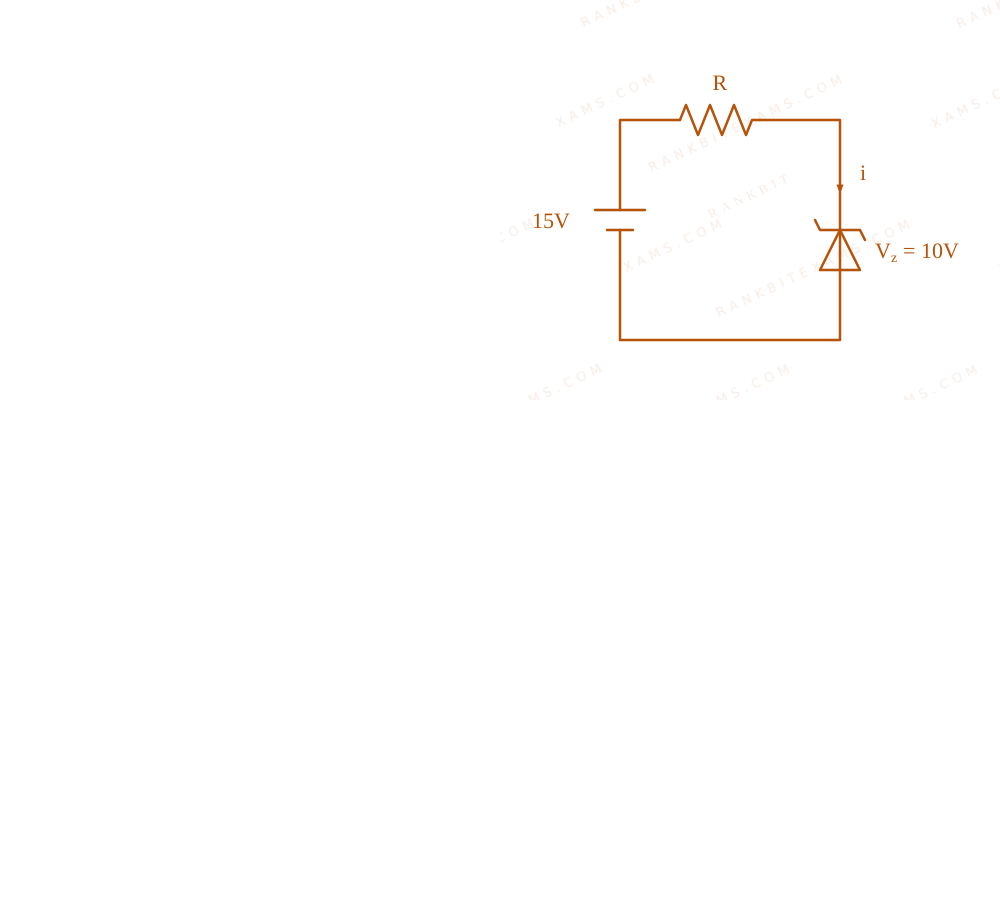
Zener diode voltage regulator circuit
The voltage drop across the series protective resistance R$R$ is:
To secure a Zener against burning out, calculate its max safe current via Pmax / Vz$P_{max} / V_z$. Feed this current into the required voltage drop (Vᵢₙ - Vz$V_{in} - V_z$) to get the exact protective resistance.
De Morgan's Laws: A · B = A + B$$\text{De Morgan's Laws: } \overline{A \cdot B} = \overline{A} + \overline{B}$$
Core Logic
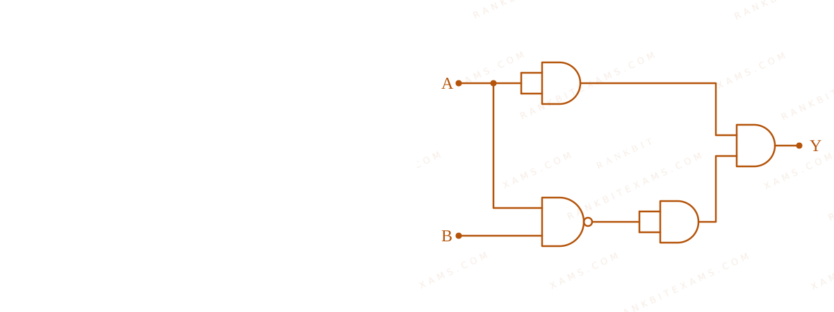
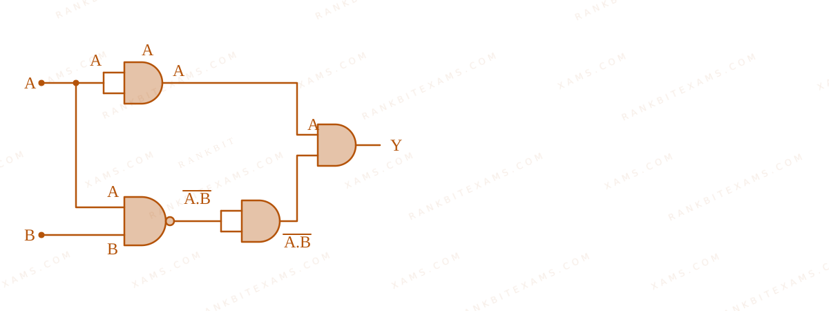
A combination of logic gates resulting in output Y.
Let's trace the logic line by line.
Top branch: A passes through an AND gate with both inputs tied to A, so it remains A$A$.
Bottom branch: A and B pass through a NAND gate, yielding A · B$\overline{A \cdot B}$. Then it passes through an AND gate with inputs tied together, so it remains A · B$\overline{A \cdot B}$.
Step 1: Boolean Expression
Finally, the inputs A$A$ and A · B$\overline{A \cdot B}$ are fed into a final AND gate.
Y = A · A · B$$Y = A \cdot \overline{A \cdot B}$$
Applying De Morgan's Law:
Y = A · ( A + B)$$Y = A \cdot (\overline{A} + \overline{B})$$Y = A · A + A · B$$Y = A \cdot \overline{A} + A \cdot \overline{B}$$
Step 2: Simplify
Since A · A = 0$A \cdot \overline{A} = 0$, we have:
Y = 0 + A B = A B$$Y = 0 + A \overline{B} = A \overline{B}$$
Checking values:
If A=1, B=0$A=1, B=0$, then Y = 1 · 1 = 1$Y = 1 \cdot 1 = 1$.
For all other combinations, Y = 0$Y = 0$.
A combination of logic gates resulting in output Y.
Pattern Recognition
An AND gate acting on A$A$ and NAND(A, B)$\text{NAND}(A, B)$ inherently acts as a "strictly A and NOT B" checker. The boolean algebra instantly simplifies A( AB)$A(\overline{AB})$ to A B$A\overline{B}$.
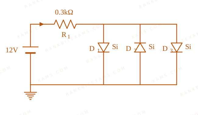
Assuming in forward bias condition there is a voltage drop of 0.7 V across a silicon diode, the current through diode D₁$D_{1}$ in the circuit is ____ mA. (Assume all diodes in the given circuit are identical)
Circuit containing a 12V source, a 0.3kOhm resistor, and three diodes D1, D2, D3 in parallel.
A.20.15$20.15$
B.11.7$11.7$
C.17.6$17.6$
D.18.8$18.8$
Solution
Related Formula
I = (V - Vd)/(R)$$I = \frac{V - V_d}{R}$$
Core Logic
Check the polarity of the battery to determine which diodes are forward-biased. Diodes D₁$D_1$ and D₂$D_2$ are forward-biased, while D₃$D_3$ is reverse-biased (acts as an open circuit). Because D₁$D_1$ and D₂$D_2$ are in parallel, the total voltage drop across the parallel combination is just 0.7 ~V$0.7 \mathrm{~V}$.
Step 1: Loop Equation
Applying KVL to the main loop containing the forward-biased diodes:
Rounding to nearest option gives 18.8 ~mA$18.8 \mathrm{~mA}$.
Pattern Recognition
Identical diodes in parallel share the current equally. The voltage drop across the entire parallel diode bank is just the drop of one diode (0.7 ~V$0.7 \mathrm{~V}$).
Chapter Mix
Class 12 Physics: Semiconductor Electronics: Materials, Devices and Simple Circuits
Q30jee_main_2026_28_january_eveningLogic Gates
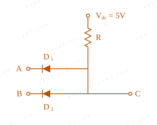
Two p-n junction diodesD₁$D_{1}$ and D₂$D_{2}$ are connected as shown in figure. A logic gate formed using two diodes connected to a 5V supply through a pull-up resistor. A and B are input signals and C is the output. The given circuit will function as a ____.
A.OR Gate$\text{OR Gate}$
B.NOR Gate$\text{NOR Gate}$
C.NAND Gate$\text{NAND Gate}$
D.AND Gate$\text{AND Gate}$
Solution
Core Logic
The circuit contains two diodes with their n-sides connected to the inputs A and B, and their p-sides tied together and connected to +5V$+5\text{V}$ through a resistor R$R$. The output C is taken from the common p-side junction.
Step 1: Analyzing the Truth Table
If either A = 0$A = 0$ (ground) or B = 0$B = 0$ (ground), the corresponding diode becomes forward biased. Current flows through the resistor R$R$, dropping the voltage at C to near 0V$0\text{V}$ (Logic 0).
If both A = 1$A = 1$ (+5V$+5\text{V}$) and B = 1$B = 1$ (+5V$+5\text{V}$), both diodes are reverse biased. No current flows through R$R$, so the voltage at C remains at +5V$+5\text{V}$ (Logic 1).
Step 2: Conclusion
The output C is 1 ONLY when both inputs A AND B are 1.
This corresponds exactly to the truth table of an AND Gate.
Pattern Recognition
Diodes pointing away from the inputs with a pull-up resistor (connected to +Vcc$+V_{cc}$) form an AND gate. If diodes point towards the inputs with a pull-down resistor to ground, it's an OR gate.
Chapter Mix
Class 12 Physics: Semiconductor Electronics: Materials, Devices and Simple Circuits
Q13jee_main_2025_02_april_eveningLogic Gates
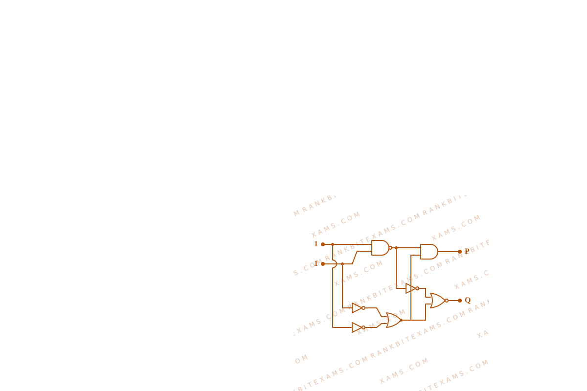
In the digital circuit shown in the figure, for the given inputs the P and Q values are :
The circuit has two inputs equal to 1, passing through multiple gates to produce outputs P and Q.
A.P = 1, Q = 1$\mathrm{P} = 1, \mathrm{Q} = 1$
B.P = 0, Q = 0$\mathrm{P} = 0, \mathrm{Q} = 0$
C.P = 0, Q = 1$\mathrm{P} = 0, \mathrm{Q} = 1$
D.P = 1, Q = 0$\mathrm{P} = 1, \mathrm{Q} = 0$
Solution
Related Formula
Truth relations of basic logic operations:
NAND operation: Y = A · B$Y = \overline{A \cdot B}$
NOR operation: Y = A + B$Y = \overline{A + B}$
NOT operation: Y = A$Y = \overline{A}$
OR operation: Y = A + B$Y = A + B$
Core Logic
The inputs are:
Top input = 1$1$
Bottom input = 1$1$
Let's analyze step-by-step from left to right:
First Gate (NAND gate at the top-left):
Inputs are 1$1$ and 1$1$.
Output = 1 · 1 = 0$\overline{1 \cdot 1} = 0$.
Bottom-left path with NOT gates:
Top input (1$1$) goes to a NOT gate, producing 0$0$.
Bottom input (1$1$) goes to a NOT gate, producing 0$0$.
These two 0$0$ values feed into the OR gate:
Output = 0 + 0 = 0$0 + 0 = 0$.
Step 1: Calculate output P
Now trace the path to P$P$:
The inputs to the top-right AND gate are:
Output of the top-left NAND gate = 0$0$
Output of the bottom-left OR gate = 0$0$
Therefore, output P$P$ is:
P = 0 · 0 = 0$$P = 0 \cdot 0 = 0$$
Step 2: Calculate output Q
Now trace the path to Q$Q$:
The gate at the bottom-right is a NOR gate with two inputs:
Input 1: Output of the top-left NAND gate (0$0$) inverted by a NOT gate = 0 = 1$\overline{0} = 1$.
Input 2: Output of the bottom-left OR gate (0$0$).
Passing these inputs (1$1$ and 0$0$) through the final NOR gate:
Sees: Combinational trace with inverted nodes.
Trap: Missing bubbles (NOT gates) representing inversion on internal circuit paths.
Shortcut: The first NAND gate output is 0$0$ (since both inputs are 1). This 0$0$ directly goes to the upper AND gate, immediately guaranteeing output P = 0$P = 0$ (eliminates options 1 and 4). Now, you only need to evaluate Q$Q$ to choose between options 2 and 3.
Chapter Mix
Class 12 Physics: Semiconductor Electronics: Materials, Devices and Simple Circuits
More Semiconductor Electronics: Materials, Devices and Simple Circuits Questions — jee_main_2025_24_jan_morning
Practice past-year questions one chapter at a time. Pick an exam → subject → chapter and get every PYQ for that topic — pulled together from all past papers — with the chapter's key formulas alongside.