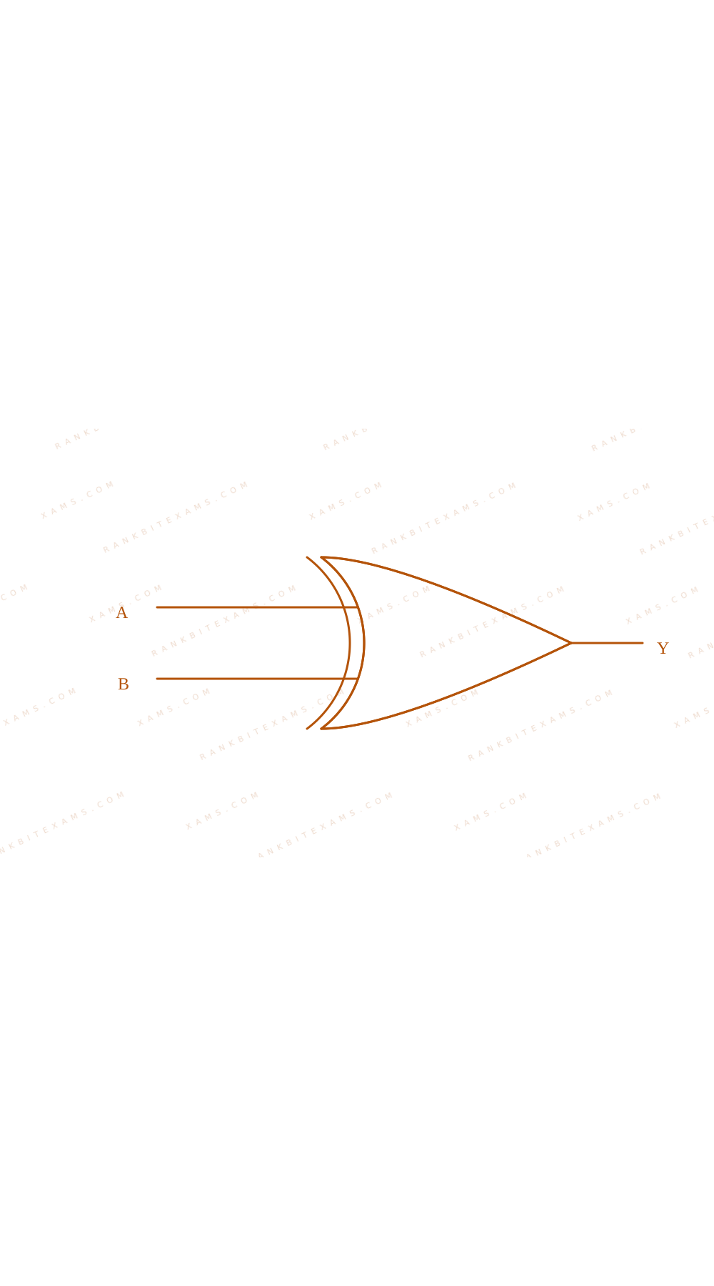
Consider the following statements: A. The junction area of solar cell is made very narrow compared to a photo diode. B. Solar cells are not connected with any external bias. C. LED is made of lightly doped p-n junction. D. Increase of forward current results in continuous increase of LED light intensity. E. LEDs have to be connected in forward bias for emission of light. Choose the correct answer from the options given below :

Solution & Explanation

Core Logic

Let's analyze each statement conceptually: Statement A: Solar cells require a wide surface layer area to intercept maximum sunlight illumination, so junction area is large.

  • Statement B: True. Solar cells operate spontaneously to provide power to loads without requiring external bias voltage.
  • Statement C: False. LEDs are made of heavily doped junctions to maximize recombination probability.
  • Statement D: False. Beyond a critical limit, high currents cause heating that drops efficiency, so emission intensity does not increase infinitely.
  • Statement E: True. Forward biasing allows minority injection leading to radiative recombination.
Step 1: Selecting Option

Since statements B and E are purely accurate, the correct grouping option is B, E Only.

Pattern Recognition

Remember: LEDs = Forward Bias, Photodiodes = Reverse Bias, Solar Cells = Zero External Bias.

Chapter Mix

Class 12 Physics: Semiconductor Electronics: Materials, Devices and Simple Circuits

Reference Study Guides

More Semiconductor Electronics: Materials, Devices and Simple Circuits Previous-Year Questions — Page 3

Q11 jee_main_2025_02_april_morning Zener Diode and Voltage Regulation
A zener diode with 5~V zener voltage is used to regulate an unregulated dc voltage input of 25~V. For a 400~Ω resistor connected in series, the zener current is found to be 4 times load current. The load current (IL) and load resistance (RL) are:
  • A. IL = 20~mA; RL = 250~Ω
  • B. IL = 10~A; RL = 0.5~Ω
  • C. IL = 0.02~mA; RL = 250~Ω
  • D. IL = 10~mA; RL = 500~Ω

Solution

Related Formula
Itotal = IZ + IL Itotal = Vᵢₙ - VZRS RL = (VZ)/(IL)
Core Logic

Given parameters:

  • Input voltage, Vᵢₙ = 25~V
  • Zener breakdown voltage, VZ = 5~V
  • Series resistor, RS = 400~Ω
  • The voltage drop across the series resistor RS is:

VRS = Vᵢₙ - VZ = 25 - 5 = 20~V

The total series current I is:

Itotal = VRSRS = (20)/(400) = 0.05~A = 50~mA

We are given that the zener current IZ is 4 times the load current IL:

IZ = 4 IL

Since Itotal = IZ + IL:

50~mA = 4 IL + IL = 5 IL IL = 10~mA

The load resistance connected in parallel with the Zener diode is:

RL = (VZ)/(IL) = 5~V10 × 10⁻³~A = 500~Ω
Step 1: Final Conclusion

The load current is 10~mA and the load resistance is 500~Ω.

Pattern Recognition

In any zener regulator problem: first determine the series path current using Itotal = Vᵢₙ - VZRₛ. Split this total current using the given ratio of IZ and IL. Finally, determine RL from VZ / IL.

Chapter Mix

Class 12 Physics: Semiconductor Electronics
Q jee_main_2025_03_april_evening Logic Gates and Truth Tables
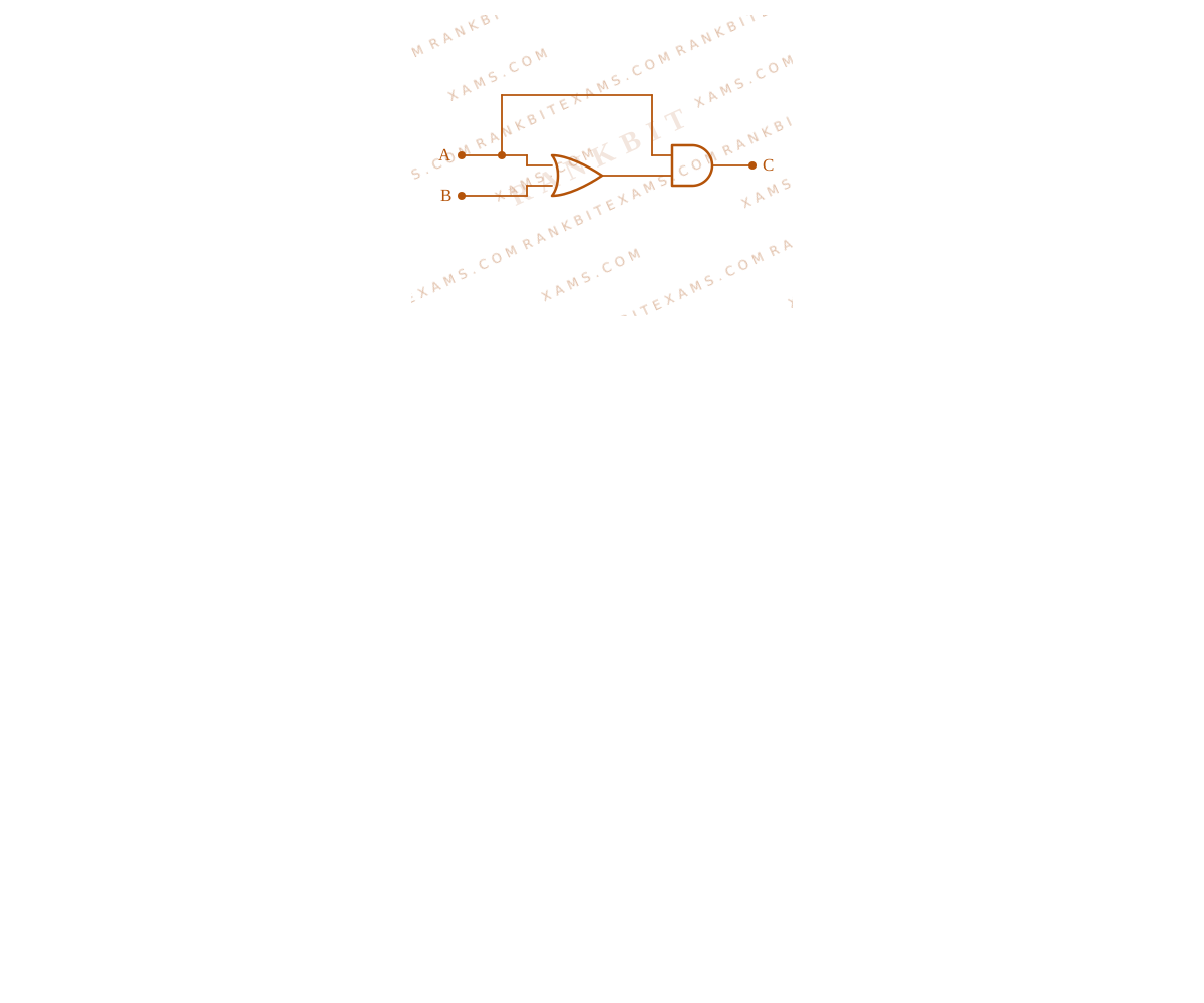
The truth table corresponding to the circuit given below is:
Logic gate circuit diagram for Q13 - JEE Main 2025 Evening
Diagram showing a combination of logic gates connected to inputs A and B resulting in output C.
  • A. Table 1
  • B. Table 2
  • C. Table 3
  • D. Table 4

Solution

Related Formula

Boolean operators for basic logic gates:

  • OR gate:
  • Y = A + B

  • AND gate:
  • Y = A · B

Core Logic

Analyze the schematic:

  • Input lines A and B are linked into an OR gate, yielding output:
  • Y = A + B

  • This term A + B and the original input line A form the inputs to a final AND gate.
  • The final output expression C is therefore:
C = A · (A + B)

Logic Gates and Truth Tables
Diagram showing a combination of logic gates connected to inputs A and B resulting in output C.

Step 1: Construct the Truth Table

Compute output values for each input combination:

  • For A=0, B=0:
C = 0 · (0 + 0) = 0
  • For A=1, B=0:
C = 1 · (1 + 0) = 1 · 1 = 1
  • For A=0, B=1:
C = 0 · (0 + 1) = 0 · 1 = 0
  • For A=1, B=1:
C = 1 · (1 + 1) = 1 · 1 = 1

This matches Table 2.

Pattern Recognition

Using Boolean algebra:

C = A · (A + B) = A · A + A · B = A + A · B

By absorption law:

A + A · B = A

So the circuit is equivalent to a simple buffer carrying input A. The output C must match input A under all conditions. Checking the options, Table 2 is the one where output C tracks input A directly (0, 1, 0, 1).

Chapter Mix

Class 12 Physics: Semiconductors

Q jee_main_2025_07_april_morning Zener Diode
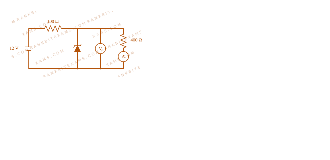
In the following circuit, the reading of the ammeter will be (Take Zener breakdown voltage = 4 V)
Zener regulator circuit for Q11 - JEE Main 2025 Morning
A schematic showing a 12V supply connected to a series 100 ohm resistor, which then branches into a parallel Zener diode and a 400 ohm resistor in series with an ammeter.
Zener regulator circuit for Q11 - JEE Main 2025 Morning
A schematic showing a 12V supply connected to a series 100 ohm resistor, which then branches into a parallel Zener diode and a 400 ohm resistor in series with an ammeter.
  • A. 24mA
  • B. 80mA
  • C. 10mA
  • D. 60mA

Solution

Related Formula

Voltage division across load RL with series resistance Rₛ without Zener regulation:

VL = Vᵢₙ ( (RL)/(Rₛ + RL) )

If VL > Vz, the Zener diode enters breakdown, and potential across the parallel load is clamped at VL = Vz.

Core Logic

Verify if Zener diode operates in the breakdown region:

  • Vᵢₙ = 12 ~V
  • Rₛ = 100 Ω
  • RL = 400 Ω
  • Calculate the unregulated voltage:

V₁ = 12 × ( (400)/(100 + 400) ) = 12 × (4)/(5) = 9.6 ~V

Since V₁ > Vz (9.6 ~V > 4 ~V), breakdown occurs, and the parallel branch voltage is fixed at Vz = 4 ~V.

Step 1: Calculate Branch Current

The voltage across the 400 Ω load resistor (which is in series with the ammeter) is locked at 4 ~V.

The current I through the ammeter is:

I = (Vz)/(RL) = 4 ~V400 Ω = 10⁻² ~A = 10 ~mA
Pattern Recognition

Sees: Parallel Zener diode configuration. Shortcut: Always calculate the open-circuit load voltage first. If it exceeds Vz, use Vz as the branch potential. The branch current is simply Vz / RL. Here, 4 / 400 = 10 ~mA.

Chapter Mix

Class 12 Physics: Semiconductor Electronics: Materials, Devices and Simple Circuits

Q8 jee_main_2025_08_april_evening Diodes
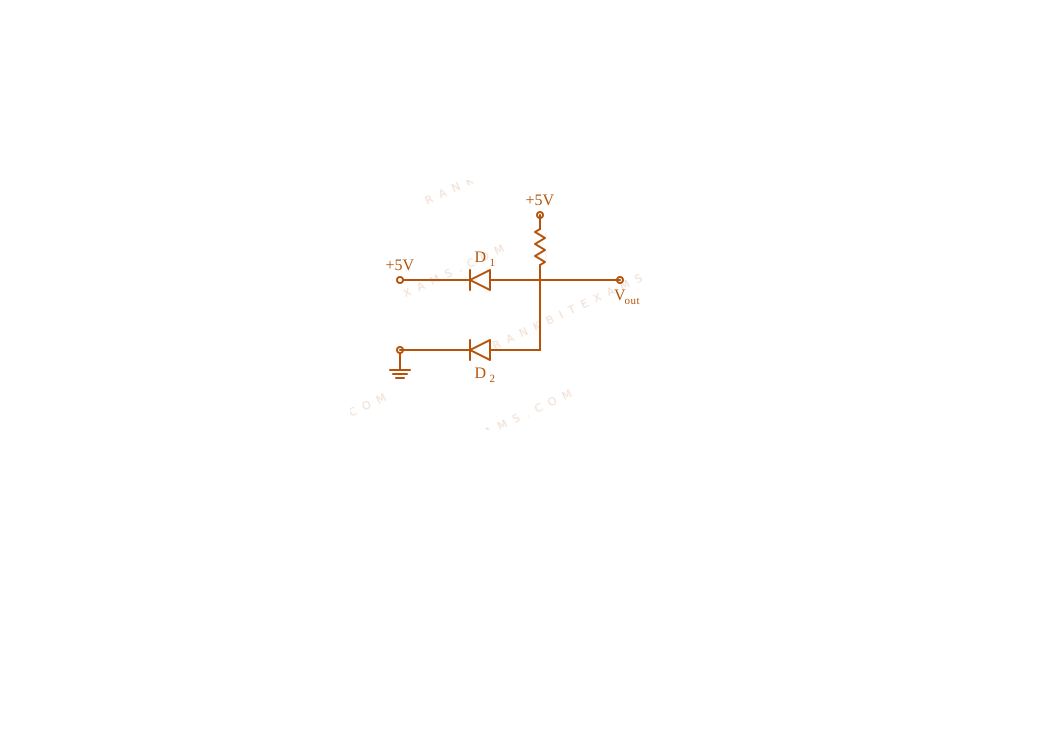
The output voltage in the following circuit is (Consider ideal diode case)
Diodes circuit diagram for Q8 - JEE Main 2025 Evening
A schematic of a circuit showing an input voltage, two diodes D1 and D2 connected in parallel paths, a resistor, and the output node V_out.
  • A. 10~V
  • B. 0~V
  • C. +5~V
  • D. -5~V

Solution

Related Formula

For ideal diodes:

  • Forward Bias: Acts as a closed switch (zero resistance, short circuit).
  • Reverse Bias: Acts as an open switch (infinite resistance, open circuit).
Core Logic

Analyzing the bias condition of the diodes based on the applied potential in the schematic:

  • Diode D₁ is oriented such that its cathode faces the positive terminal (+5~V), making it Reverse Biased (no current flows through this branch).
  • Diode D₂ is oriented such that its anode connects to the +5~V path, making it Forward Biased.
  • Since D₂ is forward-biased and ideal, it acts as a short circuit (resistance RD = 0). Current flows through D₂ and through the series resistor.

Step 1: Calculating output node potential

Because the forward-biased ideal diode D₂ connects the node directly to the low-resistance ground loop or the reference resistor drop, the entire 5~V potential drops across the resistor:

Vout = 0~V
Pattern Recognition

Sees: Parallel diode configuration with opposite polarities. Shortcut: Check polarity. D₁ is reverse-biased (open), D₂ is forward-biased (short). The output terminal is pulled down to the reference ground, leading directly to 0~V. ✓

Chapter Mix

Class 12 Physics: Semiconductor Electronics

Q18 jee_main_2025_29_jan_evening Logic Gates
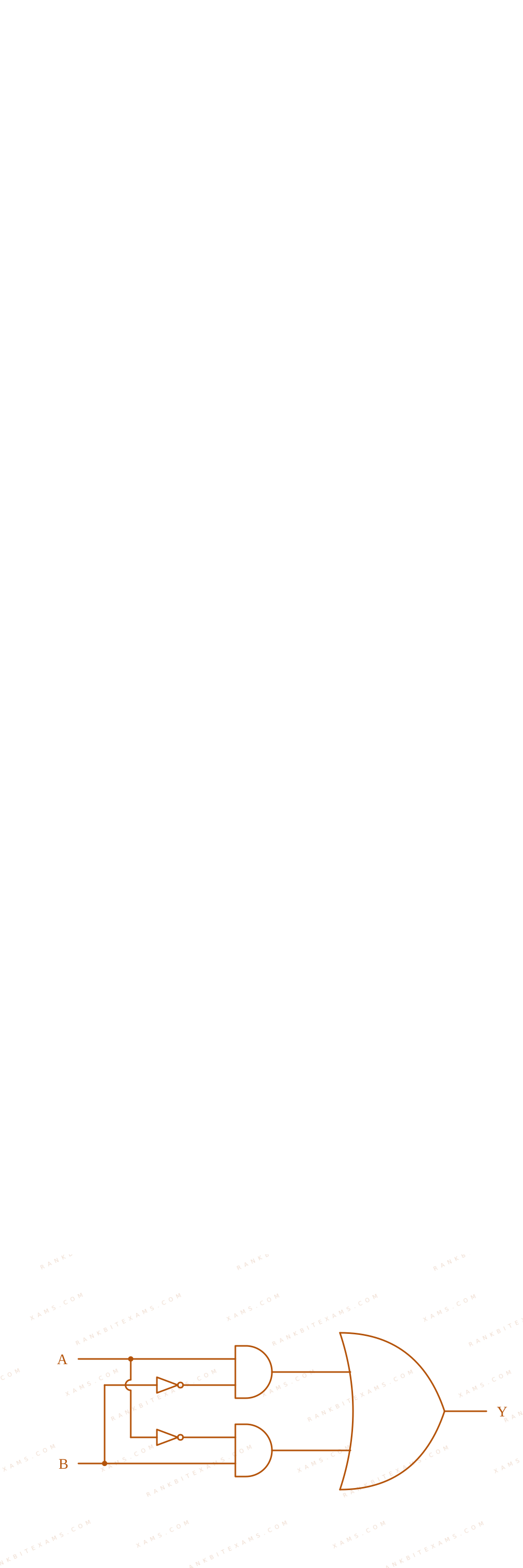
The truth table for the circuit given below is :
Logic Gates circuit diagram for Q18 - JEE Main 2025 Evening
The image shows a digital logic circuit containing multiple interconnected logic gates with input terminals A and B and output terminal Y.
  • A. array|c|c|c| A & B & Y 0 & 0 & 0 0 & 1 & 1 1 & 0 & 1 1 & 1 & 0 array
  • B. array|c|c|c| A & B & Y 0 & 0 & 0 1 & 0 & 0 1 & 1 & 0 0 & 1 & 1 array
  • C. array|c|c|c| A & B & Y 0 & 0 & 0 1 & 0 & 1 0 & 1 & 0 1 & 1 & 0 array
  • D. array|c|c|c| A & B & Y 0 & 0 & 0 1 & 1 & 1 1 & 0 & 1 0 & 1 & 1 array

Solution

Related Formula
Y = A · B + A · B = A B
Core Logic

Analyzing the circuit layout:

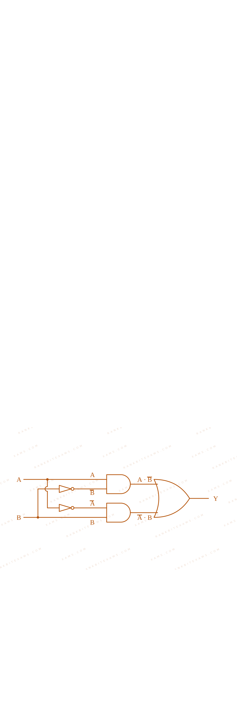
  • The top AND gate receives inputs A and B, yielding output term A B.
  • The bottom AND gate receives inputs A and B, yielding output term AB.
  • These terms pass into a terminal OR gate, producing:
Y = A B + AB

Logic Boolean Analysis diagram for Q18 - JEE Main 2025 Evening
The image shows a digital logic circuit containing multiple interconnected logic gates with input terminals A and B and output terminal Y.
Logic Boolean Analysis diagram for Q18 - JEE Main 2025 Evening
The image shows a digital logic circuit containing multiple interconnected logic gates with input terminals A and B and output terminal Y.

This is the precise expression for an XOR (Exclusive OR) gate. The corresponding truth table gives an output of 1 only when inputs are mismatched (0,1 or 1,0), and 0 otherwise. This aligns exactly with Option 1.

Pattern Recognition

Recognize the symmetric cross-inversion network of gates: (A · B) + ( A · B). This combination structurally builds an XOR logic function.

Chapter Mix

Class 12 Physics: Semiconductor Electronics

More Semiconductor Electronics: Materials, Devices and Simple Circuits Questions — jee_main_2025_24_jan_morning

Practice all Semiconductor Electronics: Materials, Devices and Simple Circuits previous-year questions →

Rankbit System
JEE Physics: Waves (+15.5%) | Electrostatics: Concentric Shells (-29.7%) | Modern Physics: Photoelectric Clones (+34.2%) | Mathematics: Definite Integrals (+18.1%) | Chemistry: Coordination Splitting (-11.4%) | JEE Physics: Waves (+15.5%) | Electrostatics: Concentric Shells (-29.7%) | Modern Physics: Photoelectric Clones (+34.2%) | Mathematics: Definite Integrals (+18.1%) | Chemistry: Coordination Splitting (-11.4%)