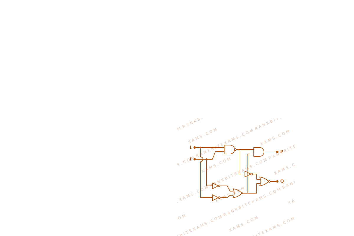
In the digital circuit shown in the figure, for the given inputs the P and Q values are :
Digital logic gate circuit diagram with inputs 1 and 1
The circuit has two inputs equal to 1, passing through multiple gates to produce outputs P and Q.

Solution & Explanation

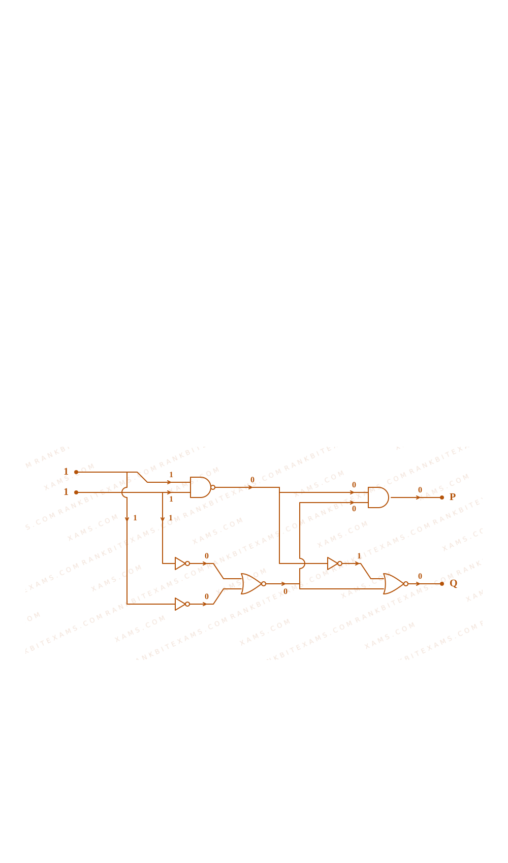
### Related Formula Truth relations of basic logic operations: - NAND operation: Y = overlineA cdot B - NOR operation: Y = overlineA + B - NOT operation: Y = overlineA - OR operation: Y = A + B ### Core Logic The inputs are: - Top input = 1 - Bottom input = 1 Let's analyze step-by-step from left to right: 1. **First Gate (NAND gate at the top-left):** - Inputs are 1 and 1. - Output = overline1 cdot 1 = 0. 2. **Bottom-left path with NOT gates:** - Top input (1) goes to a NOT gate, producing 0. - Bottom input (1) goes to a NOT gate, producing 0. - These two 0 values feed into the OR gate: - Output = 0 + 0 = 0. ### Step 1: Calculate output P Now trace the path to P: - The inputs to the top-right AND gate are: - Output of the top-left NAND gate = 0 - Output of the bottom-left OR gate = 0 - Therefore, output P is: P = 0 cdot 0 = 0 ### Step 2: Calculate output Q Now trace the path to Q: - The gate at the bottom-right is a NOR gate with two inputs: - Input 1: Output of the top-left NAND gate (0) inverted by a NOT gate = overline0 = 1. - Input 2: Output of the bottom-left OR gate (0). - Passing these inputs (1 and 0) through the final NOR gate: Q = overline1 + 0 = overline1 = 0 Thus, both P = 0 and Q = 0. ### Pattern Recognition Sees: Combinational trace with inverted nodes. Trap: Missing bubbles (NOT gates) representing inversion on internal circuit paths. Shortcut: The first NAND gate output is 0 (since both inputs are 1). This 0 directly goes to the upper AND gate, immediately guaranteeing output P = 0 (eliminates options 1 and 4). Now, you only need to evaluate Q to choose between options 2 and 3. ### Evaluation Rubric / Model Answer null ### Chapter Mix Class 12 Physics: Semiconductor Electronics: Materials, Devices and Simple Circuits
Step-by-step digital logic state values annotated on the circuit diagram
The circuit has two inputs equal to 1, passing through multiple gates to produce outputs P and Q.

Reference Study Guides

More Semiconductor Electronics: Materials, Devices and Simple Circuits Previous-Year Questions — Page 3

Q6 jee_main_2025_24_jan_morning Optoelectronic Junction Devices
Consider the following statements: A. The junction area of solar cell is made very narrow compared to a photo diode. B. Solar cells are not connected with any external bias. C. LED is made of lightly doped p-n junction. D. Increase of forward current results in continuous increase of LED light intensity. E. LEDs have to be connected in forward bias for emission of light. Choose the correct answer from the options given below :
  • A. B, D, E Only
  • B. A, C Only
  • C. A, C, E Only
  • D. B, E Only

Solution

### Core Logic Let's analyze each statement conceptually: Statement A: Solar cells require a wide surface layer area to intercept maximum sunlight illumination, so junction area is large. * Statement B: True. Solar cells operate spontaneously to provide power to loads without requiring external bias voltage. * Statement C: False. LEDs are made of heavily doped junctions to maximize recombination probability. * Statement D: False. Beyond a critical limit, high currents cause heating that drops efficiency, so emission intensity does not increase infinitely. * Statement E: True. Forward biasing allows minority injection leading to radiative recombination. ### Step 1: Selecting Option Since statements B and E are purely accurate, the correct grouping option is B, E Only. ### Pattern Recognition Remember: LEDs = Forward Bias, Photodiodes = Reverse Bias, Solar Cells = Zero External Bias. ### Evaluation Rubric / Model Answer null ### Chapter Mix Class 12 Physics: Semiconductor Electronics: Materials, Devices and Simple Circuits
Q15 jee_main_2025_28_jan_evening Diode Rectifiers
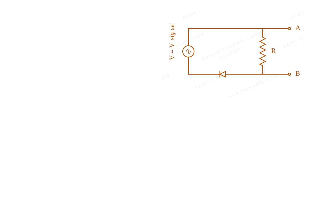
In the circuit shown here, assuming threshold voltage of diode is negligibly small, then voltage mathrmV_AB is correctly represented by:
Diode Rectifiers diagram for Q15 - JEE Main 2025 Evening
An AC source connected across an orientation circuit involving an ideal junction diode.
  • A. mathrmV_ABtext would be zero at all times
  • B. {{IMG_OPT2}}
  • C. {{IMG_OPT3}}
  • D. {{IMG_OPT4}}

Solution

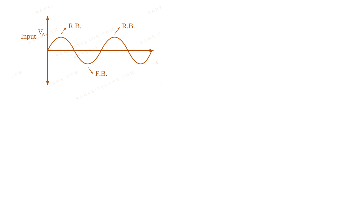
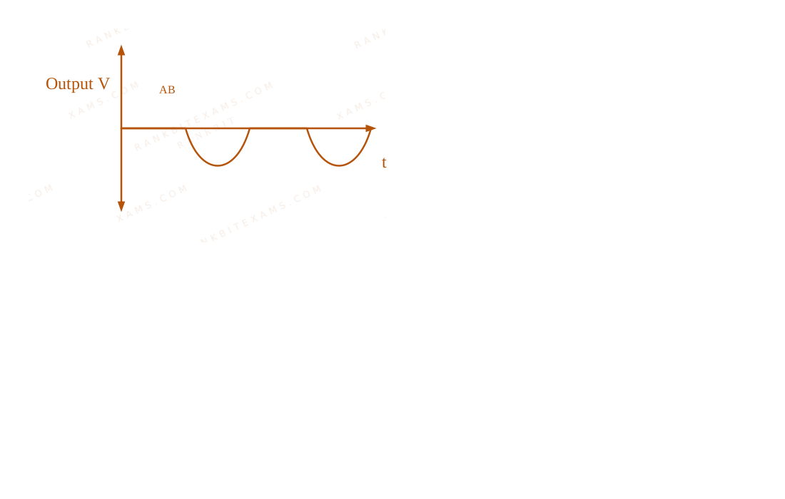
### Core Logic Analyze the cycle profile behavior of the input voltage waveform V = V_0 sin omega t: 1. **Positive Half Cycle**: Node A achieves a positive potential relative to node B. Under this configuration, the diode enters a **Reverse Biased (R.B.)** state, acting as an open switch circuit block. Since no current conducts across the resistive path, the potential difference tracked directly mirrors the input wave voltage. 2. **Negative Half Cycle**: Node A goes negative relative to node B. This transitions the diode into a **Forward Biased (F.B.)** condition, acting as a closed short-circuit bypass path. Consequently, the potential settles down immediately to zero. This behavior is visualized through the input/output tracking waveforms below:
Diode Rectifiers solution step diagram for Q15
An AC source connected across an orientation circuit involving an ideal junction diode.
Diode Rectifiers solution step diagram for Q15
An AC source connected across an orientation circuit involving an ideal junction diode.
### Step 1: Selection Matching this half-wave rectified configuration precisely selects option (4). ### Pattern Recognition When solving diode waveform problems, replace the diode mentally with an open circuit during reverse bias and a short circuit during forward bias to quickly observe the resulting output profile. ### Evaluation Rubric / Model Answer null ### Chapter Mix Class 12 Physics: Semiconductor Electronics
Q jee_main_2025_29_jan_morning Logic Gates
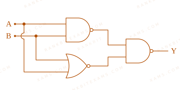
Logic Gates diagram for Q15 - JEE Main 2025 Morning
The image features a digital circuit blueprint constructed from basic logic gates with inputs A and B mapped to an output Y.
For the circuit shown above, equivalent GATE is :
Logic Gates diagram for Q15 - JEE Main 2025 Morning
The image features a digital circuit blueprint constructed from basic logic gates with inputs A and B mapped to an output Y.
  • A. OR gate
  • B. NOT gate
  • C. AND gate
  • D. NAND gate

Solution

### Core Logic Evaluating the given logic gate diagram combination step-by-step for all input permutations yields the following truth table :
Input AInput BOutput Y
000
011
101
111
This behavior matches an OR Gate configuration perfectly. ### Chapter Mix Class 12 Physics: Semiconductor Electronics
Q33 jee_main_2024_01_february_morning Zener Diode
In the given circuit if the power rating of Zener diode is 10mathrm~mW, the value of series resistance R_s to regulate the input unregulated supply is:
Zener Diode voltage regulation circuit for Q33 - JEE Main 2024 Morning
The diagram illustrates a Zener diode stabilizer network with an unregulated input supply of 8V, a Zener voltage of 5V, a series resistor Rs, and a load resistor RL of 1 kOhm.
  • A. 5mathrm~kOmega
  • B. 10mathrm~Omega
  • C. 1mathrm~kOmega
  • D. 10mathrm~kOmega

Solution

### Related Formula Voltage drop across series resistor: V_s = V_textin - V_Z Load current: I_L = fracV_ZR_L Maximum Zener current: I_Ztextmax = fracP_ZV_Z ### Core Logic Given values: V_textin = 8mathrm~V, V_Z = 5mathrm~V, R_L = 1mathrm~kOmega, P_Z = 10mathrm~mW. Voltage across R_s: V_R_s = 8 - 5 = 3mathrm~V Current through the load resistor: I_L = frac51 times 10^3 = 5mathrm~mA Maximum current allowed through the Zener diode: I_Ztextmax = frac10 times 10^-35 = 2mathrm~mA ### Step 1: Determine the Range of Resistance Total current through the series loop: I_s = I_Z + I_L For maximum safety configuration (Zener operating at peak current): I_stextmax = I_Ztextmax + I_L = 2mathrm~mA + 5mathrm~mA = 7mathrm~mA R_stextmin = fracV_R_sI_stextmax = frac3mathrm~V7mathrm~mA = frac37mathrm~kOmega approx 428.6mathrm~Omega For minimum Zener current requirement (I_Z to 0): I_stextmin = 0 + 5mathrm~mA = 5mathrm~mA R_stextmax = fracV_R_sI_stextmin = frac3mathrm~V5mathrm~mA = frac35mathrm~kOmega = 600mathrm~Omega Therefore, the required window for regulation is: frac37mathrm~kOmega < R_s < frac35mathrm~kOmega ### Step 2: Note on Official Key None of the given multiple-choice options fall strictly within the stable bounds [428.6mathrm~Omega, 600mathrm~Omega]. Officially, the answer key evaluates option (3) as correct, though the problem functions fundamentally as a bonus candidate under rigorous design tolerances. ### Pattern Recognition Always solve the current constraints at both boundaries (I_Z = 0 and I_Z = I_textmax) to bracket the allowable series resistor zone. ### Evaluation Rubric / Model Answer null ### Chapter Mix Class 12 Physics: Semiconductor Electronics
Q37 jee_main_2024_27_jan_morning Diode Biasing
  • A. Circuit Schematic A
  • B. Circuit Schematic B
  • C. Circuit Schematic C
  • D. Circuit Schematic D

Solution

### Core Logic For a p-n junction diode to be reverse-biased, the p-side must be connected to a lower electrical potential relative to the n-side. Evaluating option (4): The p-side is at -10text V and the n-side is at +2text V. Since V_p < V_n, this circuit is explicitly reverse-biased. ### Pattern Recognition Always calculate V_p - V_n. If Delta V < 0, it is reverse biasing; if Delta V > 0, it is forward biasing. ### Evaluation Rubric / Model Answer null ### Chapter Mix Class 12 Physics: Semiconductor Electronics

More Semiconductor Electronics: Materials, Devices and Simple Circuits Questions — jee_main_2025_02_april_evening
Practice all Semiconductor Electronics: Materials, Devices and Simple Circuits previous-year questions →
Rankbit System
JEE Physics: Waves (+15.5%) | Electrostatics: Concentric Shells (-29.7%) | Modern Physics: Photoelectric Clones (+34.2%) | Mathematics: Definite Integrals (+18.1%) | Chemistry: Coordination Splitting (-11.4%) | JEE Physics: Waves (+15.5%) | Electrostatics: Concentric Shells (-29.7%) | Modern Physics: Photoelectric Clones (+34.2%) | Mathematics: Definite Integrals (+18.1%) | Chemistry: Coordination Splitting (-11.4%)
