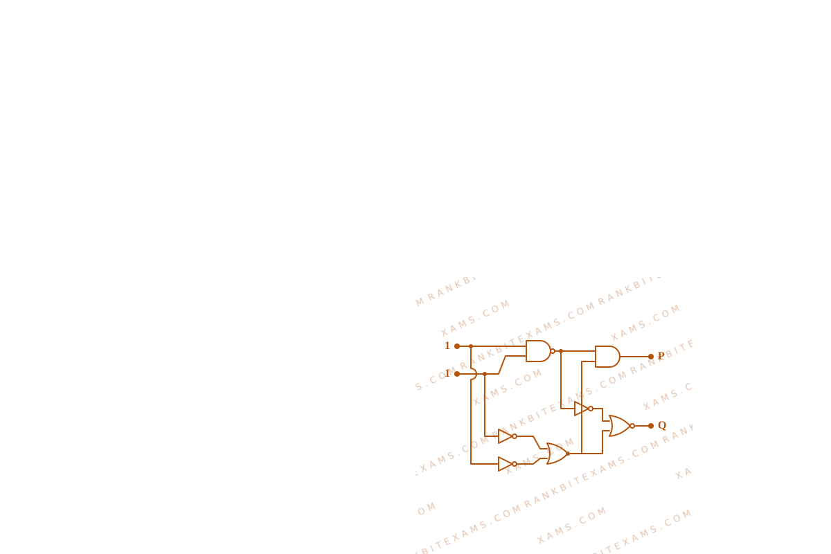
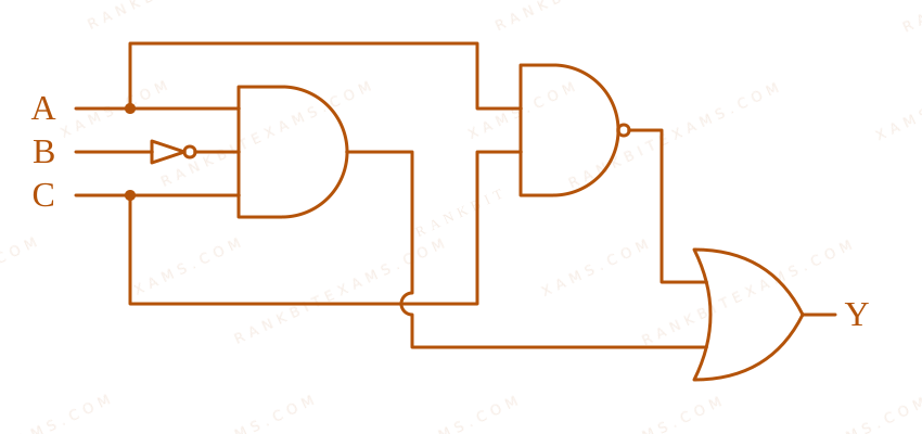
In the digital circuit shown in the figure, for the given inputs the P and Q values are :
The circuit has two inputs equal to 1, passing through multiple gates to produce outputs P and Q.
### Related Formula
Truth relations of basic logic operations:
- NAND operation: Y = overlineA cdot B$Y = \overline{A \cdot B}$
- NOR operation: Y = overlineA + B$Y = \overline{A + B}$
- NOT operation: Y = overlineA$Y = \overline{A}$
- OR operation: Y = A + B$Y = A + B$
### Core Logic
The inputs are:
- Top input = 1$1$
- Bottom input = 1$1$
Let's analyze step-by-step from left to right:
1. **First Gate (NAND gate at the top-left):**
- Inputs are 1$1$ and 1$1$.
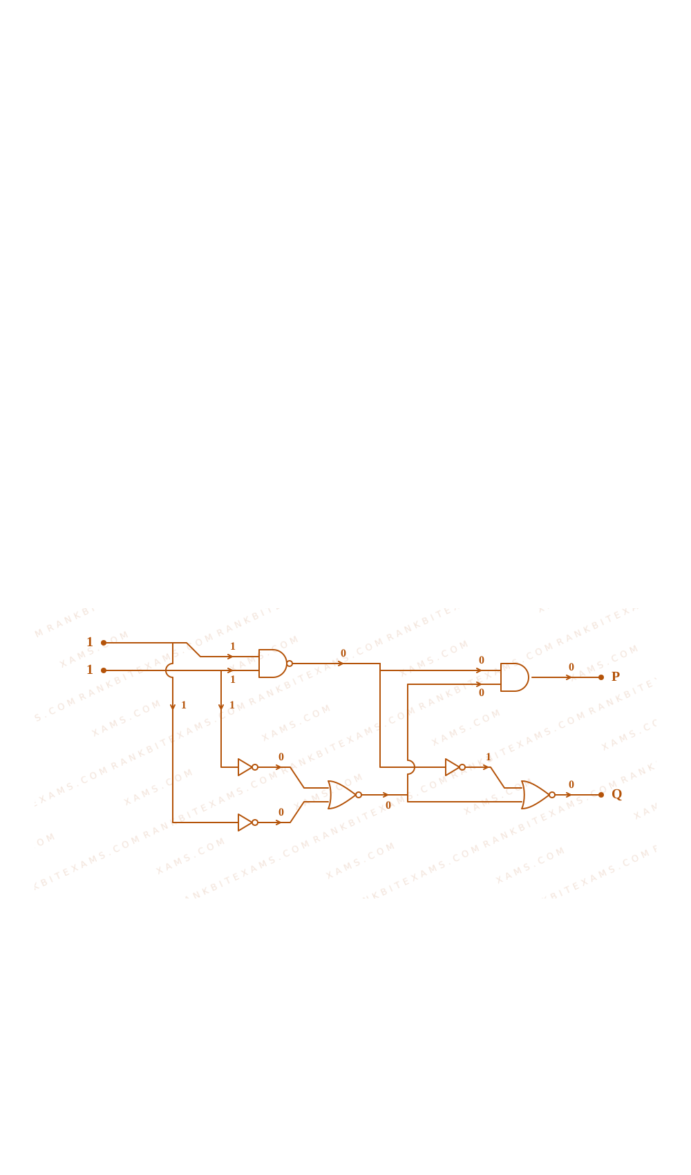
- Output = overline1 cdot 1 = 0$\overline{1 \cdot 1} = 0$.
2. **Bottom-left path with NOT gates:**
- Top input (1$1$) goes to a NOT gate, producing 0$0$.
- Bottom input (1$1$) goes to a NOT gate, producing 0$0$.
- These two 0$0$ values feed into the OR gate:
- Output = 0 + 0 = 0$0 + 0 = 0$.
### Step 1: Calculate output P
Now trace the path to P$P$:
- The inputs to the top-right AND gate are:
- Output of the top-left NAND gate = 0$0$
- Output of the bottom-left OR gate = 0$0$
- Therefore, output P$P$ is:
P = 0 cdot 0 = 0$$P = 0 \cdot 0 = 0$$
### Step 2: Calculate output Q
Now trace the path to Q$Q$:
- The gate at the bottom-right is a NOR gate with two inputs:
- Input 1: Output of the top-left NAND gate (0$0$) inverted by a NOT gate = overline0 = 1$\overline{0} = 1$.
- Input 2: Output of the bottom-left OR gate (0$0$).
- Passing these inputs (1$1$ and 0$0$) through the final NOR gate:
Q = overline1 + 0 = overline1 = 0$$Q = \overline{1 + 0} = \overline{1} = 0$$
Thus, both P = 0$P = 0$ and Q = 0$Q = 0$.
### Pattern Recognition
Sees: Combinational trace with inverted nodes.
Trap: Missing bubbles (NOT gates) representing inversion on internal circuit paths.
Shortcut: The first NAND gate output is 0$0$ (since both inputs are 1). This 0$0$ directly goes to the upper AND gate, immediately guaranteeing output P = 0$P = 0$ (eliminates options 1 and 4). Now, you only need to evaluate Q$Q$ to choose between options 2 and 3.
### Evaluation Rubric / Model Answer
null
### Chapter Mix
Class 12 Physics: Semiconductor Electronics: Materials, Devices and Simple Circuits
The circuit has two inputs equal to 1, passing through multiple gates to produce outputs P and Q.
Keywords:#logic gates digital circuit diagram#JEE Main 2025 Evening Q13#trace combinational logic circuit#Semiconductor Electronics logic gates#NAND gate#NOR gate#NOT gate#digital logic circuit
More Semiconductor Electronics: Materials, Devices and Simple Circuits Previous-Year Questions — Page 2
Q13jee_main_2025_28_jan_morningLogic Gates
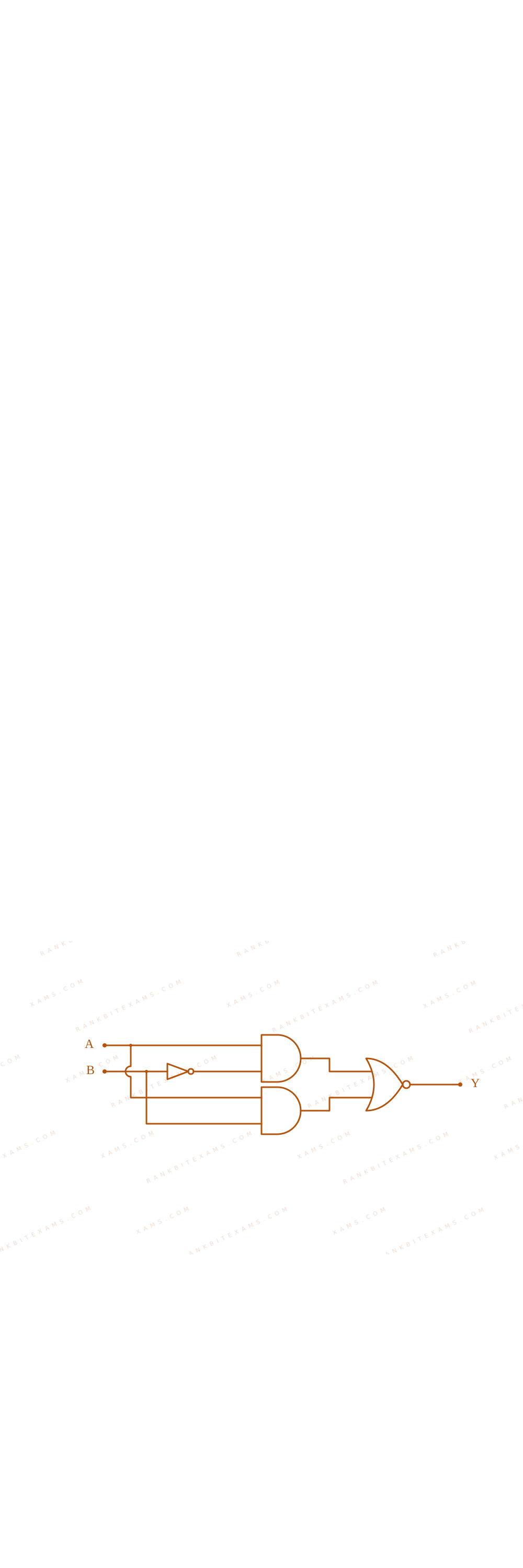
Which of the following circuits has the same output as that of the given circuit?
A combination gate circuit configuration evaluated for total Boolean output expressions.
A.textCircuit (1)$\text{Circuit (1)}$
B.textCircuit (2)$\text{Circuit (2)}$
C.textCircuit (3)$\text{Circuit (3)}$
D.textCircuit (4)$\text{Circuit (4)}$
Solution
### Core Logic
Let's perform Boolean analysis on the configuration steps mapped below:
mathrmP = mathrmA cdot barmathrmB$$\mathrm{P} = \mathrm{A} \cdot \bar{\mathrm{B}}$$mathrmQ = mathrmA cdot mathrmB$$\mathrm{Q} = \mathrm{A} \cdot \mathrm{B}$$mathrmY = overlinemathrmP + mathrmQ = overlinemathrmA cdot barmathrmB + mathrmA cdot mathrmB$$\mathrm{Y} = \overline{\mathrm{P} + \mathrm{Q}} = \overline{\mathrm{A} \cdot \bar{\mathrm{B}} + \mathrm{A} \cdot \mathrm{B}}$$
Factoring using distributive Boolean rules:
mathrmY = overlinemathrmA cdot (mathrmB + barmathrmB) = overlinemathrmA cdot 1$$\mathrm{Y} = \overline{\mathrm{A} \cdot (\mathrm{B} + \bar{\mathrm{B}})} = \overline{\mathrm{A} \cdot 1}$$mathrmY = barmathrmA$$\mathrm{Y} = \bar{\mathrm{A}}$$
### Step 1: Final Reduction
The expression reduces to a simple inverter (NOT gate) processing input A. This aligns with Circuit (1), matching option (1).
### Pattern Recognition
Identify standard combinations: (mathrmA text AND NOT mathrmB) text OR (mathrmA text AND mathrmB)$(\mathrm{A} \text{ AND NOT } \mathrm{B}) \text{ OR } (\mathrm{A} \text{ AND } \mathrm{B})$ collapses back into simply input A because operand B covers all possible states.
### Evaluation Rubric / Model Answer
null
### Chapter Mix
Class 12 Physics: Semiconductor Electronics: Materials, Devices and Simple Circuits
Q3jee_main_2025_03_april_morningLogic Gates
Choose the correct logic circuit for the given truth table having inputs A and B.
Inputs
Output
A$A$
B$B$
Y$Y$
0
0
0
0
1
0
1
0
1
1
1
1
A. Circuit (1)
B. Circuit (2)
C. Circuit (3)
D. Circuit (4)
Solution
### Related Formula
Let us inspect the Boolean expression for the output Y$Y$ from the truth table.
From the table:
- If A=0$A=0$, Y=0$Y=0$ regardless of B$B$.
- If A=1$A=1$, Y=1$Y=1$ regardless of B$B$.
Thus, the truth table is represented by the simple direct logical equation:
Y = A$Y = A$
### Core Logic
Let's check the Boolean output of the options shown in the question paper:
- **Circuit (1)**: Inputs A$A$ and B$B$ go into an OR gate, outputting (A + B)$(A + B)$. This output and B$B$ then go to an AND gate.
Y = (A + B) cdot B = Acdot B + Bcdot B = B(A + 1) = B$$Y = (A + B) \cdot B = A\cdot B + B\cdot B = B(A + 1) = B$$
This gives Y = B$Y = B$ (Not matching table).
- **Circuit (2)**: Inputs A$A$ and B$B$ go into an OR gate, outputting (A + B)$(A + B)$. This and A$A$ then go into an AND gate.
Y = (A + B) cdot A = Acdot A + Acdot B = A + Acdot B = A(1 + B) = A$$Y = (A + B) \cdot A = A\cdot A + A\cdot B = A + A\cdot B = A(1 + B) = A$$
This gives Y = A$Y = A$ (Perfect match to the truth table where Y$Y$ exactly copies A$A$).
### Step 1: Verification of Circuit (2)
Let's double-check the truth table values for Circuit (2):
- For A=0, B=0$A=0, B=0$: Y = (0 + 0) cdot 0 = 0$Y = (0 + 0) \cdot 0 = 0$.
- For A=0, B=1$A=0, B=1$: Y = (0 + 1) cdot 0 = 0$Y = (0 + 1) \cdot 0 = 0$.
- For A=1, B=0$A=1, B=0$: Y = (1 + 0) cdot 1 = 1$Y = (1 + 0) \cdot 1 = 1$.
- For A=1, B=1$A=1, B=1$: Y = (1 + 1) cdot 1 = 1$Y = (1 + 1) \cdot 1 = 1$.
This perfectly matches the given truth table. Therefore, Circuit (2) is correct.
### Pattern Recognition
Identify the logic expression directly from the truth table first! Notice that Y$Y$ is completely independent of B$B$ and strictly equals A$A$. This immediately points to any Boolean simplification that collapses to A$A$ (such as absorption law: A(A+B) = A$A(A+B) = A$).
### Evaluation Rubric / Model Answer
null
### Chapter Mix
Class 12 Physics: Semiconductor Electronics: Materials, Devices and Simple Circuits
Consider a n-type semiconductor in which n_e$n_{e}$ and n_h$n_{h}$ are number of electrons and holes, respectively.
(A) Holes are minority carriers
(B) The dopant is a pentavalent atom
(C) n_en_hne n_i^2$n_{e}n_{h}\ne n_{i}^{2}$ (where n_i$n_{i}$ is number of electrons or holes in semiconductor when it is in intrinsic form)
(D) n_en_hge n_i^2$n_{e}n_{h}\ge n_{i}^{2}$
(E) The holes are not generated due to the donors
Choose the correct answer from the options given below:
A. (A), (C), (D) only
B. (A), (C), (E) only
C. (A), (B), (E) only
D. (A), (B), (C) only
Solution
### Related Formula
Mass Action Law:
n_e cdot n_h = n_i^2$$n_e \cdot n_h = n_i^2$$
### Core Logic
Let's analyze each statement for an n-type semiconductor:
- (A) Holes are minority carriers: True, electrons are the majority carriers.
- (B) The dopant is a pentavalent atom: True (like Phosphorus, Arsenic) which provides extra free electrons.
- (C) and (D) contradict the fundamental mass action law n_e n_h = n_i^2$n_e n_h = n_i^2$, so they are False.
- (E) Holes are generated purely due to thermal excitation, not due to donor atoms: True.
### Step 1: Assemble Correct Set
Statements (A), (B), and (E) are explicitly correct.
### Pattern Recognition
Mass action law (n_e n_h = n_i^2$n_e n_h = n_i^2$) holds uniformly for both doped types at thermal equilibrium. In n-type systems, donors directly inject electrons only; holes emerge solely from thermal breakages of lattice bonds.
### Evaluation Rubric / Model Answer
null
### Chapter Mix
Class 12 Physics: Semiconductor Electronics
Q15jee_main_2025_04_april_morningLogic Gates
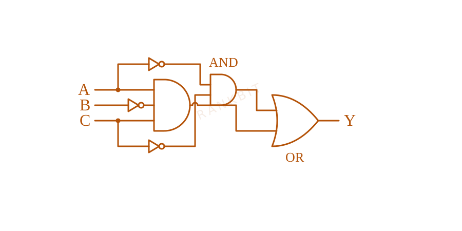
The Boolean expression Y=AoverlineBC+overlineAoverlineC$Y=Aoverline{B}C+overline{A}overline{C}$ can be realised with which of the following gate configurations.
A. One 3-input AND gate, 3 NOT gates and one 2-input OR gate, One 2-input AND gate
B. One 3-input AND gate, 1 NOT gate, One 2-input NOR gate and one 2-input OR gate
C. 3-input OR gate, 3 NOT gates and one 2-input AND gate
Choose the correct answer from the options given below
A. B, C Only
B. A, B Only
C. A, B, C Only
D. A, C Only
Solution
### Related Formula
Given logical expression:
Y = AoverlineBC + overlineAoverlineC$$Y = Aoverline{B}C + overline{A}overline{C}$$
By Boolean theorem logic:
overlineAoverlineC = overlineA+C quad text(NOR configuration)
$$overline{A}overline{C} = overline{A+C} \quad \text{(NOR configuration)}
$$
### Core Logic
Let's analyze configuration options A and B:
* **Configuration A:** Creates AoverlineBC$Aoverline{B}C$ via one 3-input AND gate and one NOT gate for B$B$. Creates overlineAoverlineC$overline{A}overline{C}$ via one 2-input AND gate and two separate NOT gates for A$A$ and C$C$. Finally combines them using a 2-input OR gate. This perfectly mirrors the terms. (Total gates: one 3-input AND, one 2-input AND, three NOT, one 2-input OR).
Logic circuit layout A for Q15 - JEE Main 2025 Morning
### Step 1: Verify Configuration B
* **Configuration B:** Creates AoverlineBC$Aoverline{B}C$ via one 3-input AND gate and one NOT gate for B$B$. Re-writes the secondary term overlineAoverlineC$overline{A}overline{C}$ into overlineA+C$overline{A+C}$, which corresponds directly to a single 2-input NOR gate. Merges both sub-tracks using a 2-input OR gate. This is also completely valid.
Logic circuit layout A for Q15 - JEE Main 2025 Morning
### Pattern Recognition
Always utilize De Morgan's identity triggers to dynamically simplify multiple product complements like overlineAoverlineC$overline{A}overline{C}$ into unified NOR formats.
### Evaluation Rubric / Model Answer
null
### Chapter Mix
Class 12 Physics: Semiconductor Electronics
Q15jee_main_2025_24_jan_eveningLogic Gates
The output of the circuit is low (zero) for : The figure contains a digital combination logic gate configuration with input variables X and Y.
(A) X = 0, Y = 0
(B) X = 0, Y = 1
(C) X = 1, Y = 0
(D) X = 1, Y = 1
Choose the correct answer from the options given below:
A. (A), (C) and (D) only
B. (A), (B) and (C) only
C. (B), (C) and (D) only
D. (A), (B) and (D) only
Solution
### Core Logic
Let us check the gate outputs row-by-row to find the boolean expression or map the truth table values: The figure contains a digital combination logic gate configuration with input variables X and Y.beginarrayccc X & Y & textOutput \hline 0 & 0 & 1 \ 0 & 1 & 0 \ 1 & 0 & 0 \ 1 & 1 & 0 endarray$$\begin{array}{ccc} X & Y & \text{Output} \\hline 0 & 0 & 1 \ 0 & 1 & 0 \ 1 & 0 & 0 \ 1 & 1 & 0 \end{array}$$
The output is low (zero) for configurations (B) X=0, Y=1$X=0, Y=1$, (C) X=1, Y=0$X=1, Y=0$, and (D) X=1, Y=1$X=1, Y=1$. Therefore, options (B), (C) and (D) only are correct.
### Pattern Recognition
The truth table profile matches a standard NOR logic configuration where the output is 1 only when all input lines are completely low.
### Evaluation Rubric / Model Answer
null
### Chapter Mix
Class 12 Physics: Semiconductor Electronics
More Semiconductor Electronics: Materials, Devices and Simple Circuits Questions — jee_main_2025_02_april_evening
We Map Every Repeating Question in Competitive Exams.
Say goodbye to generic mock test fatigue. RankBit uses smart analysis to group past exam questions into their foundational Repeating Question Types. Find chapter weightage, track repeating questions, and score higher with targeted practice.
Select Your Target Exam
Choose an exam track below to find formulas per chapter and patterns.
Syncing Exam Intelligence
Mapping formulas and patterns across all tracks…
PATH A — FULL LENGTH PRACTICE
Full Mock Test Hub
Simulate real NTA exam conditions with fully tracked mocks. Time yourself against past papers.
Practice past-year questions one chapter at a time. Pick an exam → subject → chapter and get every PYQ for that topic — pulled together from all past papers — with the chapter's key formulas alongside.
 "logic gate truth table, nand nor gates combinational, digital electronics output")
 "logic gate truth table, nand nor gates combinational, digital electronics output")
