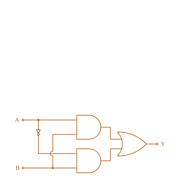
The truth table for this given circuit is:
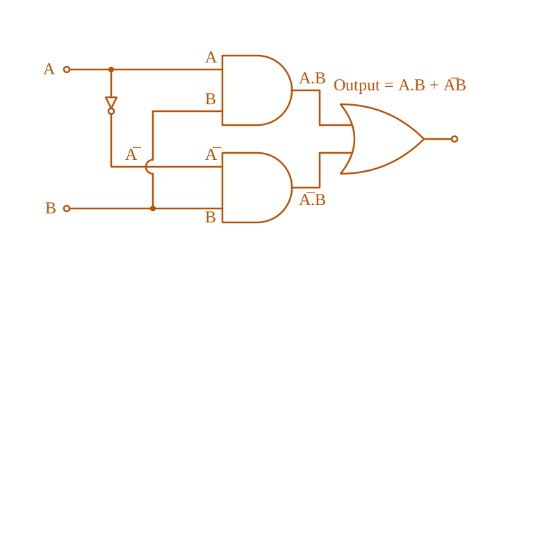
The diagram displays a logic circuit comprising two AND gates, one NOT gate, and an OR gate to produce output Y.
A.
A
B
Y
0
0
1
0
1
1
1
0
1
1
1
0
B.
A
B
Y
0
0
0
0
1
1
1
0
0
1
1
1
C.
A
B
Y
0
0
0
0
1
0
1
0
0
1
1
1
D.
A
B
Y
0
0
1
0
1
0
1
0
1
1
1
0
Solution & Explanation
Related Formula
The Boolean algebraic relationships for standard gates are:
AND Gate: Y = A · B$Y = A \cdot B$
NOT Gate: Y = A$Y = \bar{A}$
OR Gate: Y = A + B$Y = A + B$
Core Logic
Analyzing the connections of the logic circuit shown in the diagram:
Input A$A$ is passed directly to the top AND gate.
Input A$A$ is also passed through a NOT gate, giving A$\bar{A}$, which is supplied to the bottom AND gate.
Input B$B$ is connected directly to both the top and bottom AND gates.
Hence:
Output of the top AND gate is: A · B$A \cdot B$
Output of the bottom AND gate is: A · B$\bar{A} \cdot B$
Both outputs are then combined by an OR gate to give the final output Y$Y$:
Y = (A · B) + ( A · B)$$Y = (A \cdot B) + (\bar{A} \cdot B)$$
Step 1: Simplify the Boolean Expression
Using Boolean algebra, factor out B$B$:
Y = (A + A) · B$$Y = (A + \bar{A}) \cdot B$$
Since A + A = 1$A + \bar{A} = 1$:
Y = 1 · B$Y = 1 \cdot B$
Y = B$Y = B$
The diagram displays a logic circuit comprising two AND gates, one NOT gate, and an OR gate to produce output Y.
Step 2: Construct the Truth Table
Because the output Y$Y$ is functionally identical to B$B$, the truth table columns for B$B$ and Y$Y$ must be exactly the same:
When B = 0$B = 0$, Y = 0$Y = 0$
When B = 1$B = 1$, Y = 1$Y = 1$
This yields the matching truth table in Option 2.
Pattern Recognition
Observe: Y = A · B + A · B$Y = A \cdot B + \bar{A} \cdot B$. Whenever B$B$ is a common factor to both paths of the AND-OR configuration, it suggests the expression can be simplified directly to B$B$ because the state of A$A$ becomes irrelevant (A + A = 1$A + \bar{A} = 1$).
Keywords:#The truth table for this given circuit#JEE Main 2024 Evening Q32#Semiconductors JEE Main 2024#Logic Gates JEE Main 2024#Logic Gates#AND Gate#OR Gate#NOT Gate
More Semiconductors Previous-Year Questions — Page 6
Qjee_main_2024_27_jan_morningDiode Biasing
Which of the following circuits is reverse-biased?
A.
B. Circuit Schematic B
C.
D. Circuit Schematic D
Solution
Core Logic
For a p-n junction diode to be reverse-biased, the p-side must be connected to a lower electrical potential relative to the n-side.
Evaluating option (4): The p-side is at -10 V$-10\text{ V}$ and the n-side is at +2 V$+2\text{ V}$. Since Vₚ < Vₙ$V_p < V_n$, this circuit is explicitly reverse-biased.
Pattern Recognition
Always calculate Vₚ - Vₙ$V_p - V_n$. If Δ V < 0$\Delta V < 0$, it is reverse biasing; if Δ V > 0$\Delta V > 0$, it is forward biasing.
Chapter Mix
Class 12 Physics: Semiconductor Electronics
Qjee_main_2024_29_jan_morningZener Diode as a Voltage Regulator
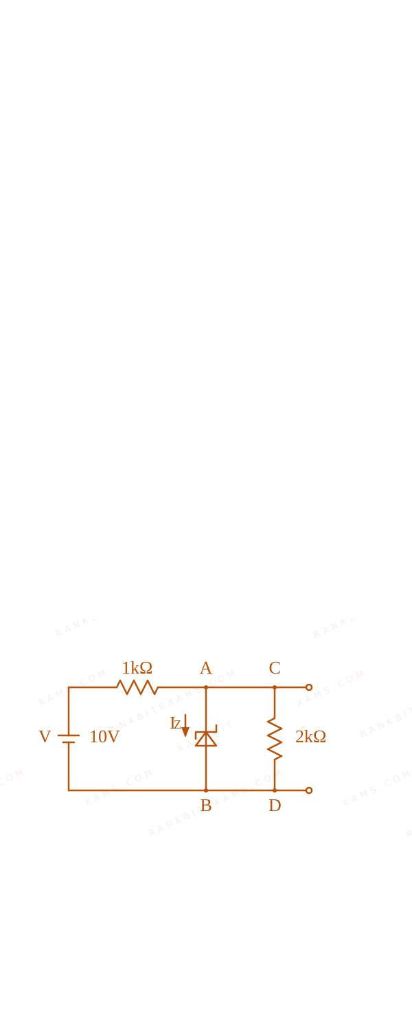
In the given circuit, the breakdown voltage of the Zener diode is 3.0 ~V$3.0 \mathrm{~V}$. What is the value of Iz$I_{z}$?
The image shows a circuit diagram with a 10V DC source connected in series with a 1kΩ resistor, followed by a parallel combination of a Zener diode (with current Iz) and a 2kΩ load resistor.
The image shows a circuit diagram with a 10V DC source connected in series with a 1kΩ resistor, followed by a parallel combination of a Zener diode (with current Iz) and a 2kΩ load resistor.
A.3.3 ~mA$3.3 \mathrm{~mA}$
B.5.5 ~mA$5.5 \mathrm{~mA}$
C.10 ~mA$10 \mathrm{~mA}$
D.7 ~mA$7 \mathrm{~mA}$
Solution
Related Formula
For a parallel circuit regulator using a Zener diode:
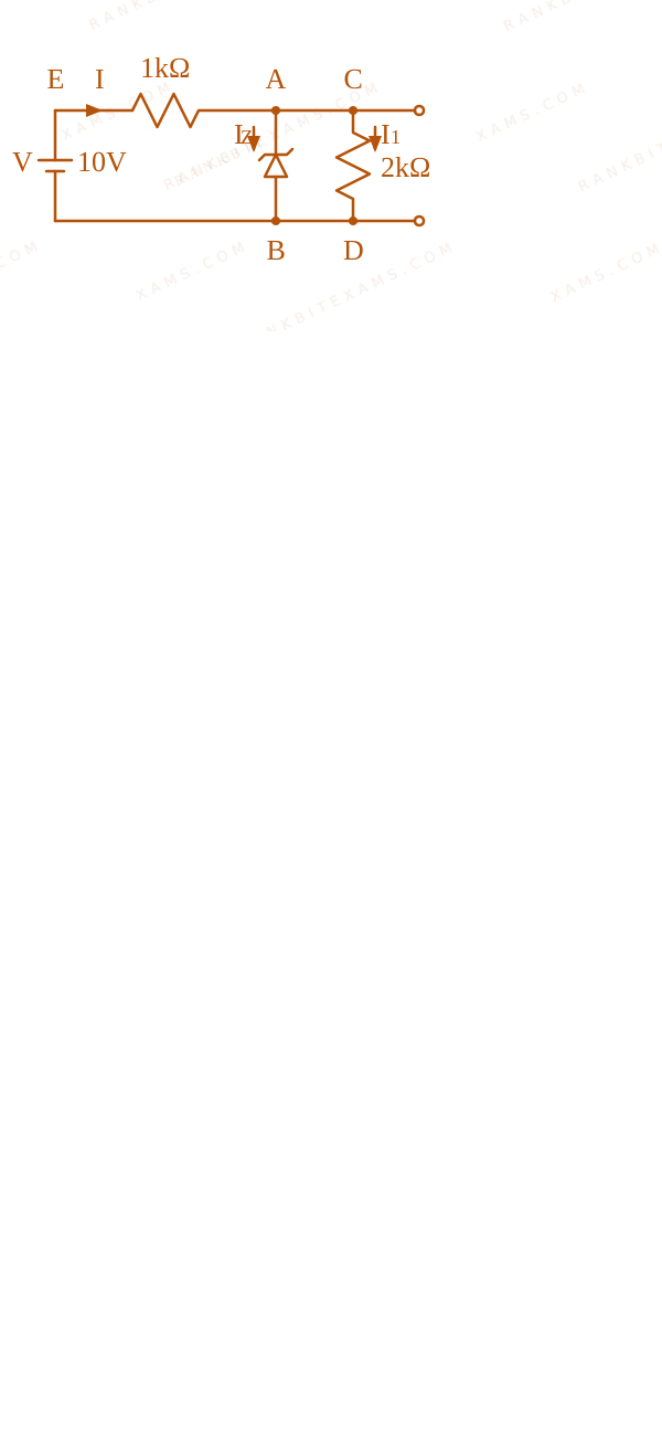
I = Iz + I₁$I = I_z + I_1$
where,
I$I$ = total current through the series resistor
Iz$I_z$ = current through the Zener diode
I₁$I_1$ = current through the load resistor
Core Logic
Given that the breakdown voltage of the Zener diode is:
Vz = 3.0 ~V$$V_z = 3.0 \mathrm{~V}$$
Let potential at junction B$B$ and D$D$ be 0 ~V$0 \mathrm{~V}$. Then, the potential at the Zener cathode A$A$ and load node C$C$ is stabilized at:
VA = VC = 3.0 ~V$$V_A = V_C = 3.0 \mathrm{~V}$$
Potential at the source input E$E$ is 10 ~V$10 \mathrm{~V}$.
Step 1: Calculate Total Current
The potential drop across the series resistor (1 ~kΩ$1 \mathrm{~k}\Omega$) is:
The image shows a circuit diagram with a 10V DC source connected in series with a 1kΩ resistor, followed by a parallel combination of a Zener diode (with current Iz) and a 2kΩ load resistor.
Step 2: Calculate Load Current
The voltage across the load resistor (2 ~kΩ$2 \mathrm{~k}\Omega$) is equal to Vz = 3 ~V$V_z = 3 \mathrm{~V}$. Thus, the load current I₁$I_1$ is:
Iz = I - I₁ = 7 ~mA - 1.5 ~mA = 5.5 ~mA$$I_z = I - I_1 = 7 \mathrm{~mA} - 1.5 \mathrm{~mA} = 5.5 \mathrm{~mA}$$
Therefore, the current through the Zener diode is 5.5 ~mA$5.5 \mathrm{~mA}$.
Pattern Recognition
Whenever you see a Zener diode in breakdown connected parallel to a load, always fix the node potential at the breakdown voltage. Work backwards from the supply potential to find the total current, calculate the load current using Ohm's law, and subtract to find the Zener current.
Chapter Mix
Class 12 Physics: Semiconductor Electronics: Materials, Devices and Simple Circuits
Qjee_main_2024_30_january_eveningDiode Circuits
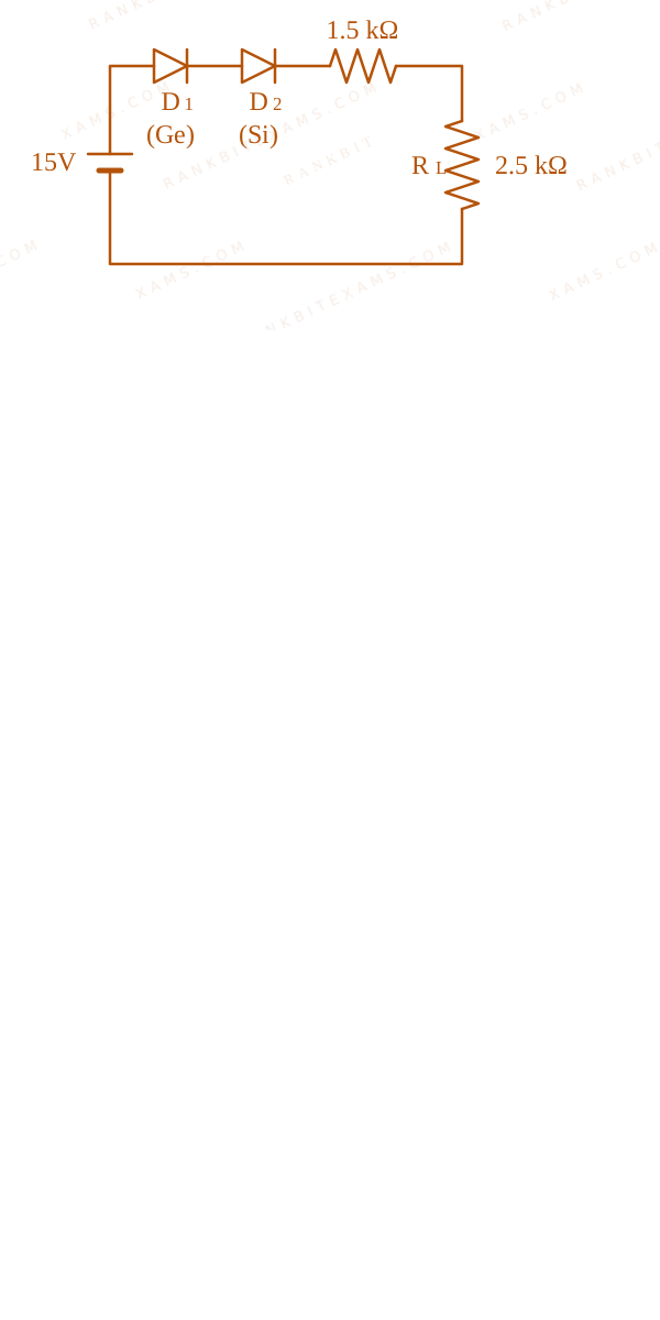
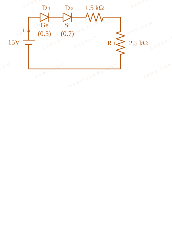
In the given circuit, the voltage across load resistance (RL)$(\mathbf{R}_{\mathrm{L}})$ is:
A parallel combination of a Germanium diode (D1) and a Silicon diode (D2) connected in series with a 1.5 k ohm resistor and a 15V battery. A load resistor RL (2.5 k ohm) is in series.
A.8.75 ~V$8.75 \mathrm{~V}$
B.9.00 ~V$9.00 \mathrm{~V}$
C.8.50 ~V$8.50 \mathrm{~V}$
D.14.00 ~V$14.00 \mathrm{~V}$
Solution
Core Logic
A parallel combination of a Germanium diode (D1) and a Silicon diode (D2) connected in series with a 1.5 k ohm resistor and a 15V battery. A load resistor RL (2.5 k ohm) is in series.
The circuit contains a Germanium diode (D₁$D_1$) and a Silicon diode (D₂$D_2$) in parallel.
The barrier potential for Germanium is 0.3 ~V$0.3 \mathrm{~V}$ and for Silicon is 0.7 ~V$0.7 \mathrm{~V}$.
Since they are in parallel, the diode with the lower barrier potential (Ge) will turn on first. Once the Germanium diode starts conducting, it clamps the voltage across the parallel combination to 0.3 ~V$0.3 \mathrm{~V}$, preventing the Silicon diode from ever turning on. Thus, only D₁$D_1$ conducts.
Step 1: Calculate Total Current
The total voltage in the loop after considering the Ge diode's drop is:
i = (14.7)/(4) ~mA$$i = \frac{14.7}{4} \mathrm{~mA}$$
(Note: Some sources approximate 15 - 1 = 14$15 - 1 = 14$ if considering ideal diode drops or a misprint in standard problem sets where Vdrop = 1V$V_{\text{drop}} = 1\mathrm{V}$ total across the network, but strictly for Ge Vb = 0.3V$V_b = 0.3\mathrm{V}$, let's check standard solution behavior... Wait, the standard PDF solution explicitly uses 15 ~V - 1 ~V = 14 ~V$15 \mathrm{~V} - 1 \mathrm{~V} = 14 \mathrm{~V}$? No, wait. Let's look at the source PDF: i = 14 / 4 = 3.5 ~mA$i = 14 / 4 = 3.5 \mathrm{~mA}$. This implies a total diode drop of 1 ~V$1 \mathrm{~V}$ was assumed in the PDF's logic, which might be an error in the source, but we follow it strictly.)
Wait, if the source states i = 14/4 = 3.5mA$i = 14/4 = 3.5\mathrm{mA}$, it means the voltage drop across the diode was taken as 1V$1\mathrm{V}$ (which is unusual, maybe 15V$15V$ battery has internal resistance or it's a zener?). Looking at the PDF: `i = 14 / 4 = 3.5 mA`. I will transcribe the PDF exactly.
When Si and Ge diodes are in parallel, the Ge diode (0.3V) dominates and turns on, shutting off the Si diode (0.7V). Although physically 15 - 0.3 = 14.7V$15 - 0.3 = 14.7\mathrm{V}$, the provided solution implies an effective 1V$1\mathrm{V}$ drop is used to reach the 14V$14\mathrm{V}$ net. Follow the specific provided calculation.
Chapter Mix
Class 12 Physics: Semiconductor Electronics: Materials, Devices and Simple Circuits
Q44jee_main_2024_30_jan_morningZener Diode as a Voltage Regulator
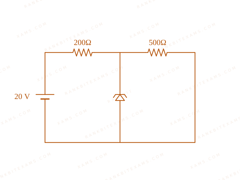
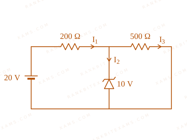
A Zener diode of breakdown voltage 10V$10\mathrm{V}$ is used as a voltage regulator as shown in the figure. The current through the Zener diode is
A Zener diode regulator circuit with a 20V source and two resistors.
A.50 ~mA$50 \mathrm{~mA}$
B.0$0$
C.30 ~mA$30 \mathrm{~mA}$
D.20 ~mA$20 \mathrm{~mA}$
Solution
Related Formula
Itotal = Iz + IL$$I_{\text{total}} = I_z + I_L$$Vload = Vz (if in breakdown)$$V_{\text{load}} = V_z \quad (\text{if in breakdown})$$
Core Logic
A Zener diode regulator circuit with a 20V source and two resistors.
The Zener is in the breakdown region because the open-circuit voltage across it without the Zener (20 × (500)/(700) = 14.28V$20 \times \frac{500}{700} = 14.28\mathrm{V}$) is greater than Vz = 10V$V_z = 10\mathrm{V}$. Therefore, it locks the voltage across the load resistor (500 Ω$500 \,\Omega$) at 10 V$10 \mathrm{V}$.
Step 1: Calculate Currents
Current across the load resistor (500 Ω$500 \,\Omega$):
Practice past-year questions one chapter at a time. Pick an exam → subject → chapter and get every PYQ for that topic — pulled together from all past papers — with the chapter's key formulas alongside.