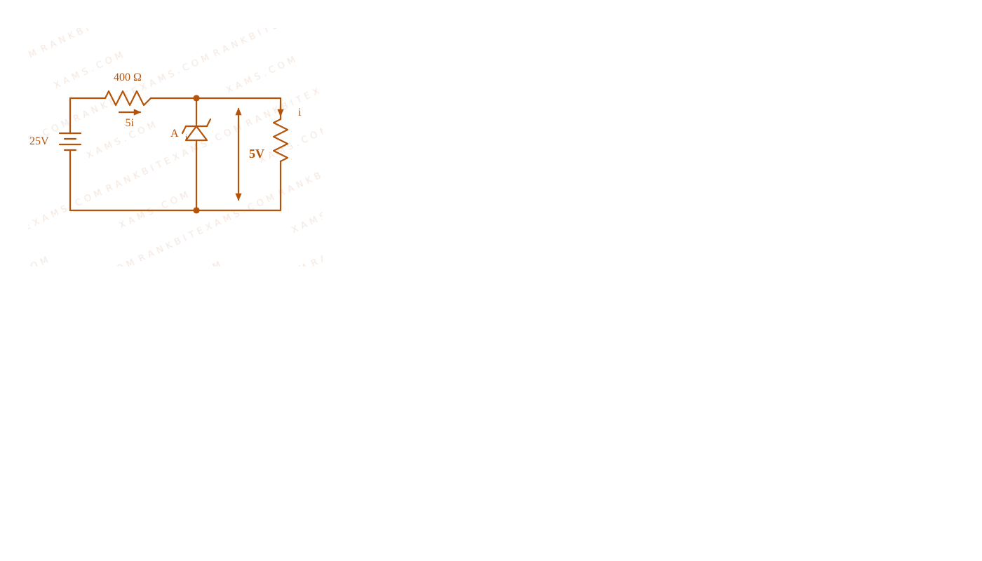
A zener diode with 5mathrm~V$5\mathrm{~V}$ zener voltage is used to regulate an unregulated dc voltage input of 25mathrm~V$25\mathrm{~V}$. For a 400mathrm~Omega$400\mathrm{~\Omega}$ resistor connected in series, the zener current is found to be 4 times load current. The load current (I_L)$(I_L)$ and load resistance (R_L)$(R_L)$ are:
### Related Formula
I_texttotal = I_Z + I_L$$I_{\text{total}} = I_Z + I_L$$I_texttotal = fracV_textin - V_ZR_S$$I_{\text{total}} = \frac{V_{\text{in}} - V_Z}{R_S}$$R_L = fracV_ZI_L$$R_L = \frac{V_Z}{I_L}$$
### Core Logic
Given parameters:
- Input voltage, V_textin = 25mathrm~V$V_{\text{in}} = 25\mathrm{~V}$
- Zener breakdown voltage, V_Z = 5mathrm~V$V_Z = 5\mathrm{~V}$
- Series resistor, R_S = 400mathrm~Omega$R_S = 400\mathrm{~\Omega}$
The voltage drop across the series resistor R_S$R_S$ is:
V_R_S = V_textin - V_Z = 25 - 5 = 20mathrm~V$$V_{R_S} = V_{\text{in}} - V_Z = 25 - 5 = 20\mathrm{~V}$$
The total series current I$I$ is:
I_texttotal = fracV_R_SR_S = frac20400 = 0.05mathrm~A = 50mathrm~mA$$I_{\text{total}} = \frac{V_{R_S}}{R_S} = \frac{20}{400} = 0.05\mathrm{~A} = 50\mathrm{~mA}$$
We are given that the zener current I_Z$I_Z$ is 4 times the load current I_L$I_L$:
I_Z = 4 I_L$I_Z = 4 I_L$
Since I_texttotal = I_Z + I_L$I_{\text{total}} = I_Z + I_L$:
50mathrm~mA = 4 I_L + I_L = 5 I_L implies I_L = 10mathrm~mA$$50\mathrm{~mA} = 4 I_L + I_L = 5 I_L \implies I_L = 10\mathrm{~mA}$$
The load resistance connected in parallel with the Zener diode is:
R_L = fracV_ZI_L = frac5mathrm~V10 times 10^-3mathrm~A = 500mathrm~Omega$$R_L = \frac{V_Z}{I_L} = \frac{5\mathrm{~V}}{10 \times 10^{-3}\mathrm{~A}} = 500\mathrm{~\Omega}$$
### Step 1: Final Conclusion
The load current is 10mathrm~mA$10\mathrm{~mA}$ and the load resistance is 500mathrm~Omega$500\mathrm{~\Omega}$.
### Pattern Recognition
In any zener regulator problem: first determine the series path current using I_texttotal = fracV_textin - V_ZR_s$I_{\text{total}} = \frac{V_{\text{in}} - V_Z}{R_s}$. Split this total current using the given ratio of I_Z$I_Z$ and I_L$I_L$. Finally, determine R_L$R_L$ from V_Z / I_L$V_Z / I_L$.
### Evaluation Rubric / Model Answer
null
### Chapter Mix
Class 12 Physics: Semiconductor Electronics
Keywords:#Zener diode voltage regulator#JEE Main 2025 Morning Q11#Semiconductors JEE Main 2025#load current and load resistance
More Semiconductors Previous-Year Questions
Qjee_main_2025_03_april_eveningLogic Gates and Truth Tables
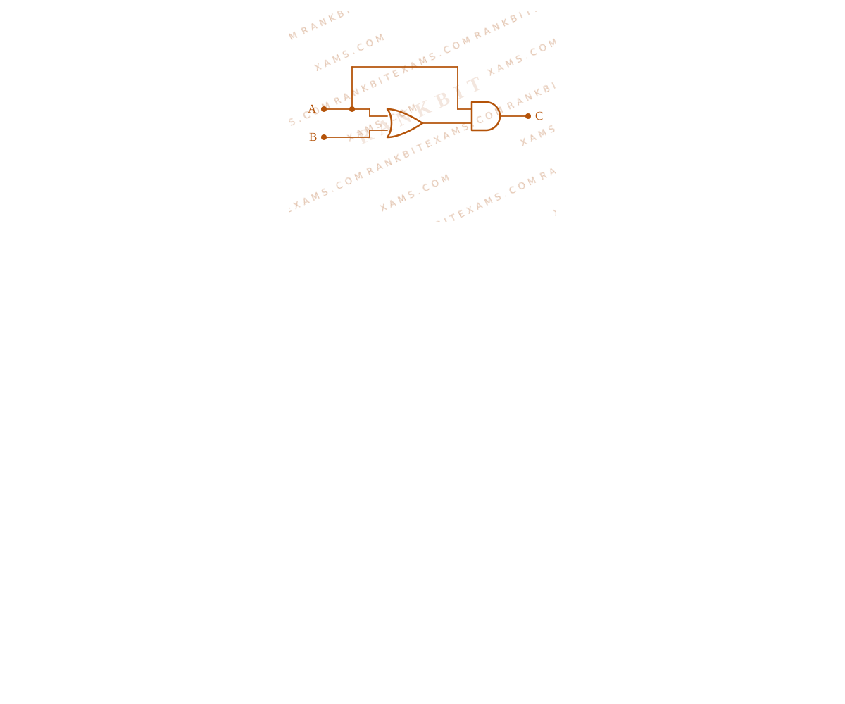
The truth table corresponding to the circuit given below is: Diagram showing a combination of logic gates connected to inputs A and B resulting in output C.
A.textTable 1$\text{Table 1}$
B.textTable 2$\text{Table 2}$
C.textTable 3$\text{Table 3}$
D.textTable 4$\text{Table 4}$
Solution
### Related Formula
Boolean operators for basic logic gates:
- OR gate:
Y = A + B$Y = A + B$
- AND gate:
Y = A cdot B$Y = A \cdot B$
### Core Logic
Analyze the schematic:
1. Input lines A$A$ and B$B$ are linked into an OR gate, yielding output:
Y = A + B$Y = A + B$
2. This term A + B$A + B$ and the original input line A$A$ form the inputs to a final AND gate.
3. The final output expression C$C$ is therefore:
C = A cdot (A + B)$$C = A \cdot (A + B)$$Diagram showing a combination of logic gates connected to inputs A and B resulting in output C.
### Step 1: Construct the Truth Table
Compute output values for each input combination:
- For A=0, B=0$A=0, B=0$:
C = 0 cdot (0 + 0) = 0$$C = 0 \cdot (0 + 0) = 0$$
- For A=1, B=0$A=1, B=0$:
C = 1 cdot (1 + 0) = 1 cdot 1 = 1$$C = 1 \cdot (1 + 0) = 1 \cdot 1 = 1$$
- For A=0, B=1$A=0, B=1$:
C = 0 cdot (0 + 1) = 0 cdot 1 = 0$$C = 0 \cdot (0 + 1) = 0 \cdot 1 = 0$$
- For A=1, B=1$A=1, B=1$:
C = 1 cdot (1 + 1) = 1 cdot 1 = 1$$C = 1 \cdot (1 + 1) = 1 \cdot 1 = 1$$
This matches Table 2.
### Pattern Recognition
Using Boolean algebra:
C = A cdot (A + B) = A cdot A + A cdot B = A + A cdot B$$C = A \cdot (A + B) = A \cdot A + A \cdot B = A + A \cdot B$$
By absorption law:
A + A cdot B = A$$A + A \cdot B = A$$
So the circuit is equivalent to a simple buffer carrying input A$A$. The output C$C$ must match input A$A$ under all conditions. Checking the options, Table 2 is the one where output C$C$ tracks input A$A$ directly (0, 1, 0, 1$0, 1, 0, 1$).
### Evaluation Rubric / Model Answer
null
### Chapter Mix
Class 12 Physics: Semiconductors
Q11jee_main_2025_07_april_eveningLogic Gates
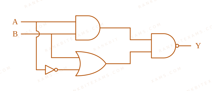
Consider the following logic circuit.
The diagram illustrates a combination of an AND gate, an inverter, an OR gate, and a terminal NAND gate with inputs A and B.
The output is Y=0$Y=0$ when : [cite: 64, 89]
A. A=1 and B=1 [cite: 90]
B. A=0 and B=1 [cite: 99]
C. A=1 and B=0 [cite: 91]
D. A=0 and B=0 [cite: 100]
Solution
### Core Logic
Let the intermediate outputs of the first layers be Y_1$Y_1$ and Y_2$Y_2$ [cite: 747]:
* Top gate is an AND gate with inputs A$A$ and B$B$, so Y_1 = A cdot B$Y_1 = A \cdot B$ [cite: 747].
* Bottom gate is an OR gate where one input is B$B$ and the other is barA$\bar{A}$ via a NOT gate, so Y_2 = barA + B$Y_2 = \bar{A} + B$ [cite: 747].
* The final layer is a NAND gate with inputs Y_1$Y_1$ and Y_2$Y_2$, so Y = overlineY_1 cdot Y_2$Y = \overline{Y_1 \cdot Y_2}$[cite: 748].
### Step 1: Constructing the Truth Table
Let's compute the output Y$Y$ for all binary input pairs (A, B)$(A, B)$ [cite: 757]:
* For A=0, B=0 implies Y_1 = 0, Y_2 = 1 implies Y = overline0 cdot 1 = 1$A=0, B=0 \implies Y_1 = 0, Y_2 = 1 \implies Y = \overline{0 \cdot 1} = 1$ [cite: 757].
* For A=1, B=0 implies Y_1 = 0, Y_2 = 0 implies Y = overline0 cdot 0 = 1$A=1, B=0 \implies Y_1 = 0, Y_2 = 0 \implies Y = \overline{0 \cdot 0} = 1$ [cite: 757].
* For A=0, B=1 implies Y_1 = 0, Y_2 = 1 implies Y = overline0 cdot 1 = 1$A=0, B=1 \implies Y_1 = 0, Y_2 = 1 \implies Y = \overline{0 \cdot 1} = 1$ [cite: 757].
* For A=1, B=1 implies Y_1 = 1, Y_2 = 1 implies Y = overline1 cdot 1 = 0$A=1, B=1 \implies Y_1 = 1, Y_2 = 1 \implies Y = \overline{1 \cdot 1} = 0$ [cite: 757].
Thus, Y=0$Y=0$ uniquely when A=1$A=1$ and B=1$B=1$[cite: 89, 90, 757].
### Pattern Recognition
A NAND gate produces an output of 0$0$ if and only if all its inputs are 1$1$. Working backward, this instantly sets Y_1=1$Y_1=1$ and Y_2=1$Y_2=1$. For Y_1 = A cdot B = 1$Y_1 = A \cdot B = 1$, we must have A=1$A=1$ and B=1$B=1$ simultaneously.
### Evaluation Rubric / Model Answer
null
### Chapter Mix
Class 12 Physics: Semiconductors
Q32jee_main_2024_29_january_eveningLogic Gates and Truth Tables
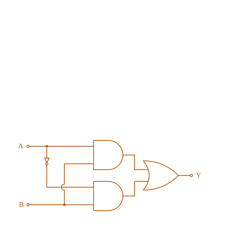
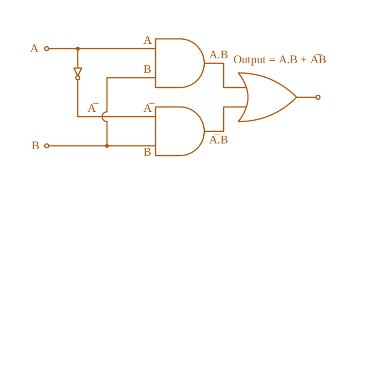
The truth table for this given circuit is:
The diagram displays a logic circuit comprising two AND gates, one NOT gate, and an OR gate to produce output Y.
A.
A
B
Y
0
0
1
0
1
1
1
0
1
1
1
0
B.
A
B
Y
0
0
0
0
1
1
1
0
0
1
1
1
C.
A
B
Y
0
0
0
0
1
0
1
0
0
1
1
1
D.
A
B
Y
0
0
1
0
1
0
1
0
1
1
1
0
Solution
### Related Formula
The Boolean algebraic relationships for standard gates are:
* AND Gate: Y = A cdot B$Y = A \cdot B$
* NOT Gate: Y = barA$Y = \bar{A}$
* OR Gate: Y = A + B$Y = A + B$
### Core Logic
Analyzing the connections of the logic circuit shown in the diagram:
1. Input A$A$ is passed directly to the top AND gate.
2. Input A$A$ is also passed through a NOT gate, giving barA$\bar{A}$, which is supplied to the bottom AND gate.
3. Input B$B$ is connected directly to both the top and bottom AND gates.
Hence:
* Output of the top AND gate is: A cdot B$A \cdot B$
* Output of the bottom AND gate is: barA cdot B$\bar{A} \cdot B$
Both outputs are then combined by an OR gate to give the final output Y$Y$:
Y = (A cdot B) + (barA cdot B)$$Y = (A \cdot B) + (\bar{A} \cdot B)$$
### Step 1: Simplify the Boolean Expression
Using Boolean algebra, factor out B$B$:
Y = (A + barA) cdot B$$Y = (A + \bar{A}) \cdot B$$
Since A + barA = 1$A + \bar{A} = 1$:
Y = 1 cdot B$Y = 1 \cdot B$Y = B$Y = B$The diagram displays a logic circuit comprising two AND gates, one NOT gate, and an OR gate to produce output Y.
### Step 2: Construct the Truth Table
Because the output Y$Y$ is functionally identical to B$B$, the truth table columns for B$B$ and Y$Y$ must be exactly the same:
* When B = 0$B = 0$, Y = 0$Y = 0$
* When B = 1$B = 1$, Y = 1$Y = 1$
This yields the matching truth table in Option 2.
### Pattern Recognition
Observe: Y = A cdot B + barA cdot B$Y = A \cdot B + \bar{A} \cdot B$. Whenever B$B$ is a common factor to both paths of the AND-OR configuration, it suggests the expression can be simplified directly to B$B$ because the state of A$A$ becomes irrelevant (A + barA = 1$A + \bar{A} = 1$).
### Evaluation Rubric / Model Answer
null
### Chapter Mix
Class 12 Physics: Semiconductors
More Semiconductors Questions — jee_main_2025_02_april_morning
We Map Every Repeating Question in Competitive Exams.
Say goodbye to generic mock test fatigue. RankBit uses smart analysis to group past exam questions into their foundational Repeating Question Types. Find chapter weightage, track repeating questions, and score higher with targeted practice.
Select Your Target Exam
Choose an exam track below to find formulas per chapter and patterns.
Syncing Exam Intelligence
Mapping formulas and patterns across all tracks…
PATH A — FULL LENGTH PRACTICE
Full Mock Test Hub
Simulate real NTA exam conditions with fully tracked mocks. Time yourself against past papers.
Practice past-year questions one chapter at a time. Pick an exam → subject → chapter and get every PYQ for that topic — pulled together from all past papers — with the chapter's key formulas alongside.
.svg "Logic gates, AND gate, OR gate, Truth table")