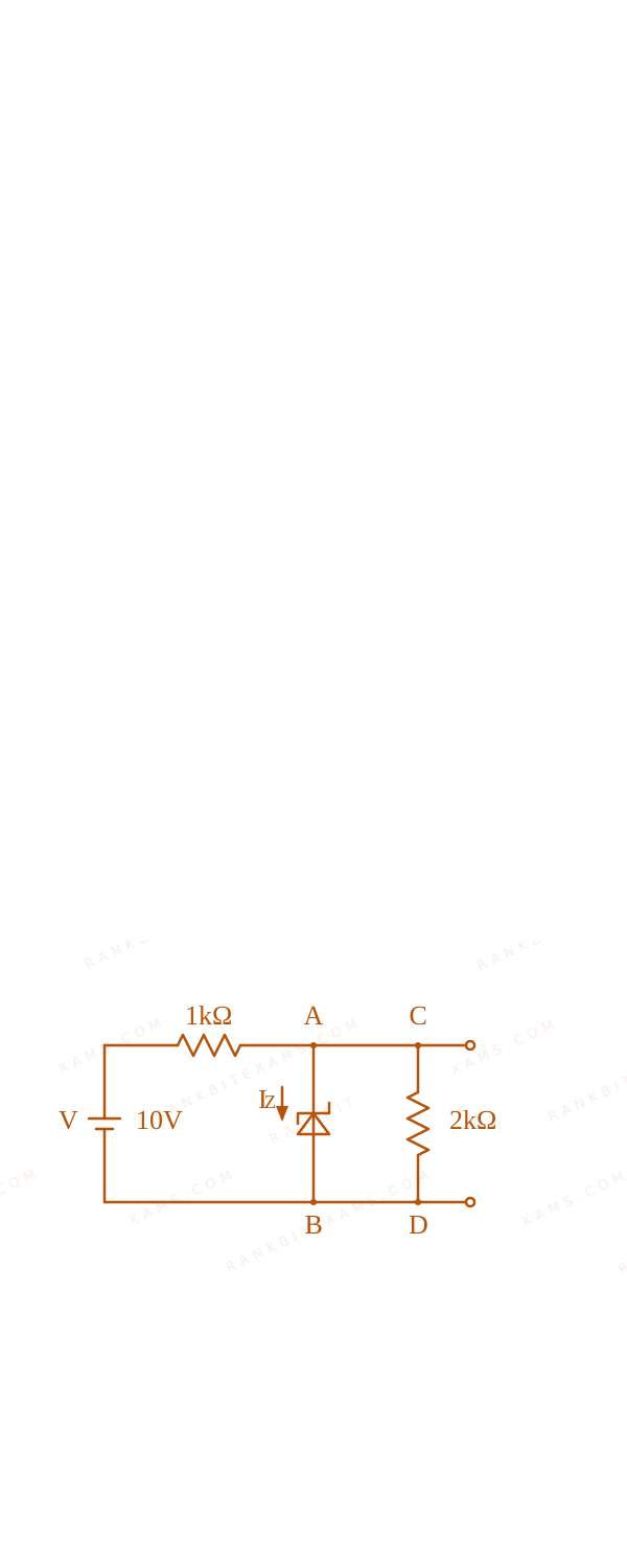
In the given circuit, the breakdown voltage of the Zener diode is 3.0 ~V$3.0 \mathrm{~V}$. What is the value of Iz$I_{z}$?
The image shows a circuit diagram with a 10V DC source connected in series with a 1kΩ resistor, followed by a parallel combination of a Zener diode (with current Iz) and a 2kΩ load resistor.
The image shows a circuit diagram with a 10V DC source connected in series with a 1kΩ resistor, followed by a parallel combination of a Zener diode (with current Iz) and a 2kΩ load resistor.
A.3.3 ~mA$3.3 \mathrm{~mA}$
B.5.5 ~mA$5.5 \mathrm{~mA}$
C.10 ~mA$10 \mathrm{~mA}$
D.7 ~mA$7 \mathrm{~mA}$
Solution & Explanation
Related Formula
For a parallel circuit regulator using a Zener diode:
I = Iz + I₁$I = I_z + I_1$
where,
I$I$ = total current through the series resistor
Iz$I_z$ = current through the Zener diode
I₁$I_1$ = current through the load resistor
Core Logic
Given that the breakdown voltage of the Zener diode is:
Vz = 3.0 ~V$$V_z = 3.0 \mathrm{~V}$$
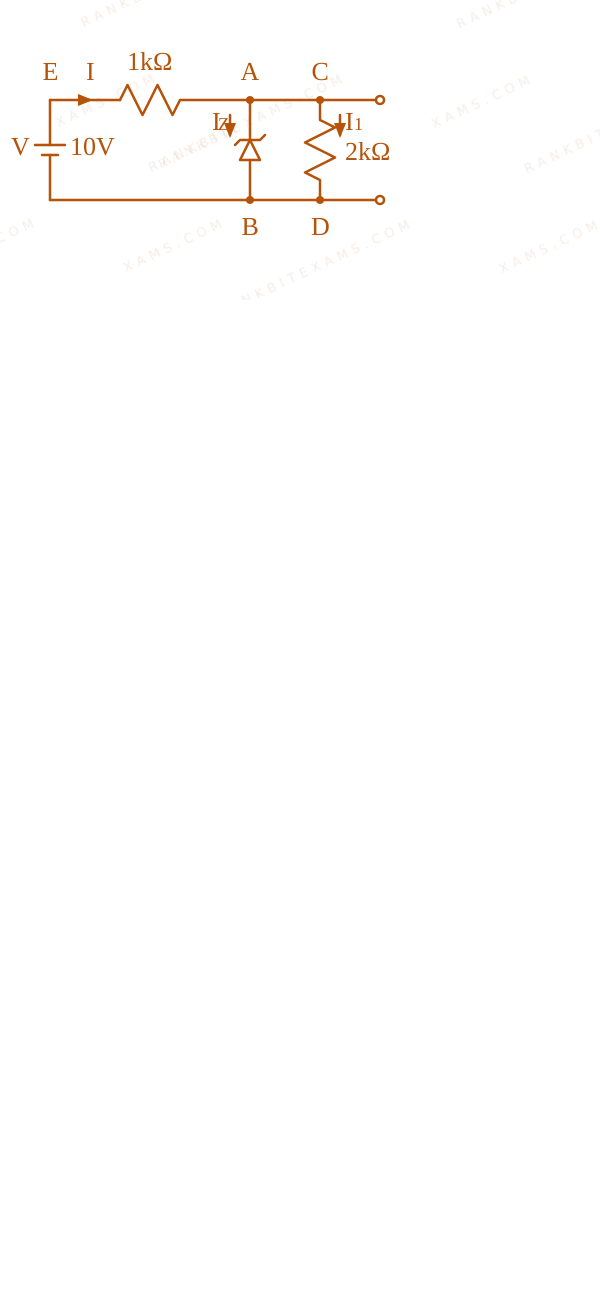
Let potential at junction B$B$ and D$D$ be 0 ~V$0 \mathrm{~V}$. Then, the potential at the Zener cathode A$A$ and load node C$C$ is stabilized at:
VA = VC = 3.0 ~V$$V_A = V_C = 3.0 \mathrm{~V}$$
Potential at the source input E$E$ is 10 ~V$10 \mathrm{~V}$.
Step 1: Calculate Total Current
The potential drop across the series resistor (1 ~kΩ$1 \mathrm{~k}\Omega$) is:
The image shows a circuit diagram with a 10V DC source connected in series with a 1kΩ resistor, followed by a parallel combination of a Zener diode (with current Iz) and a 2kΩ load resistor.
Step 2: Calculate Load Current
The voltage across the load resistor (2 ~kΩ$2 \mathrm{~k}\Omega$) is equal to Vz = 3 ~V$V_z = 3 \mathrm{~V}$. Thus, the load current I₁$I_1$ is:
Iz = I - I₁ = 7 ~mA - 1.5 ~mA = 5.5 ~mA$$I_z = I - I_1 = 7 \mathrm{~mA} - 1.5 \mathrm{~mA} = 5.5 \mathrm{~mA}$$
Therefore, the current through the Zener diode is 5.5 ~mA$5.5 \mathrm{~mA}$.
Pattern Recognition
Whenever you see a Zener diode in breakdown connected parallel to a load, always fix the node potential at the breakdown voltage. Work backwards from the supply potential to find the total current, calculate the load current using Ohm's law, and subtract to find the Zener current.
Chapter Mix
Class 12 Physics: Semiconductor Electronics: Materials, Devices and Simple Circuits
Keywords:#Zener diode#Regulator circuit#Breakdown voltage
More Semiconductor Electronics: Materials, Devices and Simple Circuits Previous-Year Questions — Page 4
Qjee_main_2025_28_jan_morningLogic Gates
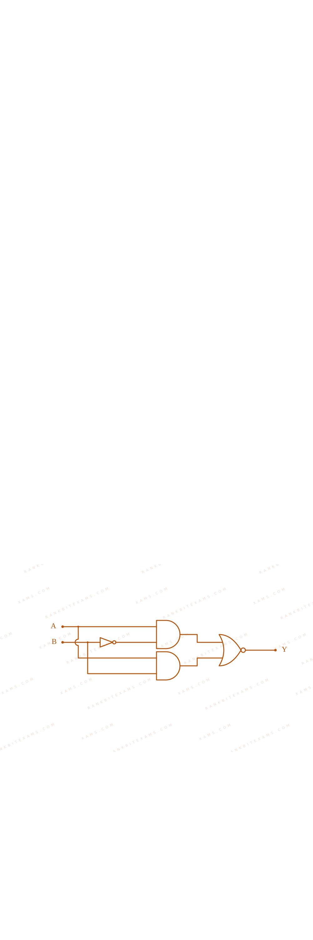
Which of the following circuits has the same output as that of the given circuit?
A combination gate circuit configuration evaluated for total Boolean output expressions.
A.
B.
C.
D.
Solution
Core Logic
Let's perform Boolean analysis on the configuration steps mapped below:
P = A · B$$\mathrm{P} = \mathrm{A} \cdot \bar{\mathrm{B}}$$Q = A · B$$\mathrm{Q} = \mathrm{A} \cdot \mathrm{B}$$Y = P + Q = A · B + A · B$$\mathrm{Y} = \overline{\mathrm{P} + \mathrm{Q}} = \overline{\mathrm{A} \cdot \bar{\mathrm{B}} + \mathrm{A} \cdot \mathrm{B}}$$
Factoring using distributive Boolean rules:
Y = A · (B + B) = A · 1$$\mathrm{Y} = \overline{\mathrm{A} \cdot (\mathrm{B} + \bar{\mathrm{B}})} = \overline{\mathrm{A} \cdot 1}$$Y = A$$\mathrm{Y} = \bar{\mathrm{A}}$$
Step 1: Final Reduction
The expression reduces to a simple inverter (NOT gate) processing input A. This aligns with Circuit (1), matching option (1).
Pattern Recognition
Identify standard combinations: (A AND NOT B) OR (A AND B)$(\mathrm{A} \text{ AND NOT } \mathrm{B}) \text{ OR } (\mathrm{A} \text{ AND } \mathrm{B})$ collapses back into simply input A because operand B covers all possible states.
Chapter Mix
Class 12 Physics: Semiconductor Electronics: Materials, Devices and Simple Circuits
Qjee_main_2025_03_april_morningLogic Gates
Choose the correct logic circuit for the given truth table having inputs A and B.
Inputs
Output
A$A$
B$B$
Y$Y$
0
0
0
0
1
0
1
0
1
1
1
1
A.
B.
C.
D.
Solution
Related Formula
Let us inspect the Boolean expression for the output Y$Y$ from the truth table.
From the table:
If A=0$A=0$, Y=0$Y=0$ regardless of B$B$.
If A=1$A=1$, Y=1$Y=1$ regardless of B$B$.
Thus, the truth table is represented by the simple direct logical equation:
Y = A$Y = A$
Core Logic
Let's check the Boolean output of the options shown in the question paper:
Circuit (1): Inputs A$A$ and B$B$ go into an OR gate, outputting (A + B)$(A + B)$. This output and B$B$ then go to an AND gate.
Y = (A + B) · B = A· B + B· B = B(A + 1) = B$$Y = (A + B) \cdot B = A\cdot B + B\cdot B = B(A + 1) = B$$
This gives Y = B$Y = B$ (Not matching table).
Circuit (2): Inputs A$A$ and B$B$ go into an OR gate, outputting (A + B)$(A + B)$. This and A$A$ then go into an AND gate.
Y = (A + B) · A = A· A + A· B = A + A· B = A(1 + B) = A$$Y = (A + B) \cdot A = A\cdot A + A\cdot B = A + A\cdot B = A(1 + B) = A$$
This gives Y = A$Y = A$ (Perfect match to the truth table where Y$Y$ exactly copies A$A$).
Step 1: Verification of Circuit (2)
Let's double-check the truth table values for Circuit (2):
This perfectly matches the given truth table. Therefore, Circuit (2) is correct.
Pattern Recognition
Identify the logic expression directly from the truth table first! Notice that Y$Y$ is completely independent of B$B$ and strictly equals A$A$. This immediately points to any Boolean simplification that collapses to A$A$ (such as absorption law: A(A+B) = A$A(A+B) = A$).
Chapter Mix
Class 12 Physics: Semiconductor Electronics: Materials, Devices and Simple Circuits
Consider a n-type semiconductor in which nₑ$n_{e}$ and nh$n_{h}$ are number of electrons and holes, respectively.
(A) Holes are minority carriers
(B) The dopant is a pentavalent atom
(C) nₑnh≠ nᵢ²$n_{e}n_{h}\ne n_{i}^{2}$ (where nᵢ$n_{i}$ is number of electrons or holes in semiconductor when it is in intrinsic form)
(D) nₑnh≥ nᵢ²$n_{e}n_{h}\ge n_{i}^{2}$
(E) The holes are not generated due to the donors
Choose the correct answer from the options given below:
A. (A), (C), (D) only
B. (A), (C), (E) only
C. (A), (B), (E) only
D. (A), (B), (C) only
Solution
Related Formula
Mass Action Law:
nₑ · nh = nᵢ²$$n_e \cdot n_h = n_i^2$$
Core Logic
Let's analyze each statement for an n-type semiconductor:
(A) Holes are minority carriers: True, electrons are the majority carriers.
(B) The dopant is a pentavalent atom: True (like Phosphorus, Arsenic) which provides extra free electrons.
(C) and (D) contradict the fundamental mass action law nₑ nh = nᵢ²$n_e n_h = n_i^2$, so they are False.
(E) Holes are generated purely due to thermal excitation, not due to donor atoms: True.
Step 1: Assemble Correct Set
Statements (A), (B), and (E) are explicitly correct.
Pattern Recognition
Mass action law (nₑ nh = nᵢ²$n_e n_h = n_i^2$) holds uniformly for both doped types at thermal equilibrium. In n-type systems, donors directly inject electrons only; holes emerge solely from thermal breakages of lattice bonds.
Chapter Mix
Class 12 Physics: Semiconductor Electronics
Qjee_main_2025_04_april_morningLogic Gates
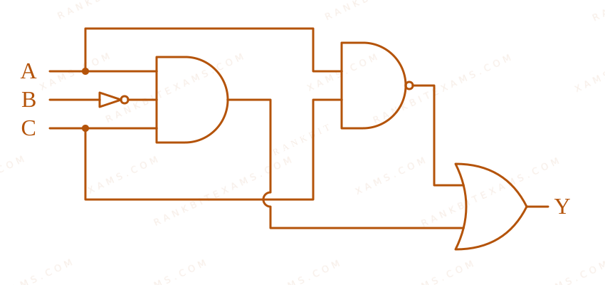
The Boolean expression Y=AoverlineBC+overlineAoverlineC$Y=Aoverline{B}C+overline{A}overline{C}$ can be realised with which of the following gate configurations.
A. One 3-input AND gate, 3 NOT gates and one 2-input OR gate, One 2-input AND gate
B. One 3-input AND gate, 1 NOT gate, One 2-input NOR gate and one 2-input OR gate
C. 3-input OR gate, 3 NOT gates and one 2-input AND gate
Choose the correct answer from the options given below
A. B, C Only
B. A, B Only
C. A, B, C Only
D. A, C Only
Solution
Related Formula
Given logical expression:
Y = A BC + A C$$Y = A\overline{B}C + \overline{A}\overline{C}$$
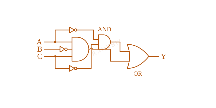
Configuration A: Generates A BC$A\overline{B}C$ using one 3-input AND gate and one NOT gate for input B$B$. Generates A C$\overline{A}\overline{C}$ using one 2-input AND gate and two separate NOT gates for inputs A$A$ and C$C$. Combines both terms using a 2-input OR gate.
(Total: one 3-input AND, one 2-input AND, three NOT gates, one 2-input OR gate).
Logic circuit layout A for Q15 - JEE Main 2025 Morning
Step 1: Verify Configuration B
Configuration B: Generates A BC$A\overline{B}C$ using one 3-input AND gate and one NOT gate for input B$B$. Simplifies the second term A C$\overline{A}\overline{C}$ into A+C$\overline{A+C}$, realized directly with a single 2-input NOR gate. Combines both sub-circuits using a 2-input OR gate.
(Total: one 3-input AND, one 2-input NOR, one NOT gate, one 2-input OR gate).
Logic circuit layout A for Q15 - JEE Main 2025 Morning
Step 2: Verify Configuration C
Configuration C: Specifies a 3-input OR gate and a 2-input AND gate at the output, which implements a product-of-sums form rather than the required sum-of-products expression. Hence, Configuration C is invalid.
Both configurations A and B correctly realize the logic function.
Pattern Recognition
Apply De Morgan's theorem (A· B = A+B$\overline{A}\cdot\overline{B} = \overline{A+B}$) to convert negated AND products into standard NOR gate structures, reducing the total gate count.
Evaluation Rubric / Model Answer
Option B: A, B Only
Chapter Mix
Class 12 Physics: Semiconductor Electronics
Q11jee_main_2025_07_april_eveningLogic Gates
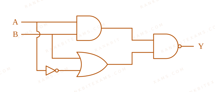
Consider the following logic circuit.
The diagram illustrates a combination of an AND gate, an inverter, an OR gate, and a terminal NAND gate with inputs A and B.
The output is Y=0$Y=0$ when : [cite: 64, 89]
A. A=1 and B=1 [cite: 90]
B. A=0 and B=1 [cite: 99]
C. A=1 and B=0 [cite: 91]
D. A=0 and B=0 [cite: 100]
Solution
Core Logic
Let the intermediate outputs of the first layers be Y₁$Y_1$ and Y₂$Y_2$ [cite: 747]:
Top gate is an AND gate with inputs A$A$ and B$B$, so Y₁ = A · B$Y_1 = A \cdot B$ [cite: 747].
Bottom gate is an OR gate where one input is B$B$ and the other is A$\bar{A}$ via a NOT gate, so Y₂ = A + B$Y_2 = \bar{A} + B$ [cite: 747].
The final layer is a NAND gate with inputs Y₁$Y_1$ and Y₂$Y_2$, so Y = Y₁ · Y₂$Y = \overline{Y_1 \cdot Y_2}$[cite: 748].
Step 1: Constructing the Truth Table
Let's compute the output Y$Y$ for all binary input pairs (A, B)$(A, B)$ [cite: 757]:
Thus, Y=0$Y=0$ uniquely when A=1$A=1$ and B=1$B=1$[cite: 89, 90, 757].
Pattern Recognition
A NAND gate produces an output of 0$0$ if and only if all its inputs are 1$1$. Working backward, this instantly sets Y₁=1$Y_1=1$ and Y₂=1$Y_2=1$. For Y₁ = A · B = 1$Y_1 = A \cdot B = 1$, we must have A=1$A=1$ and B=1$B=1$ simultaneously.
Chapter Mix
Class 12 Physics: Semiconductors
More Semiconductor Electronics: Materials, Devices and Simple Circuits Questions — jee_main_2024_29_jan_morning
Practice past-year questions one chapter at a time. Pick an exam → subject → chapter and get every PYQ for that topic — pulled together from all past papers — with the chapter's key formulas alongside.