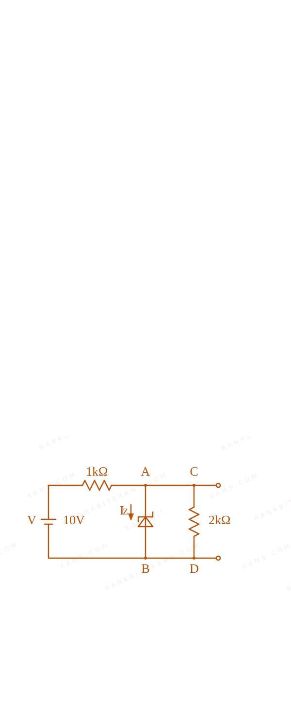
In the given circuit, the breakdown voltage of the Zener diode is 3.0 ~V$3.0 \mathrm{~V}$. What is the value of Iz$I_{z}$?
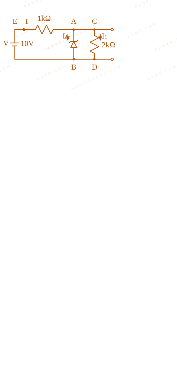
The image shows a circuit diagram with a 10V DC source connected in series with a 1kΩ resistor, followed by a parallel combination of a Zener diode (with current Iz) and a 2kΩ load resistor.
A.3.3 ~mA$3.3 \mathrm{~mA}$
B.5.5 ~mA$5.5 \mathrm{~mA}$
C.10 ~mA$10 \mathrm{~mA}$
D.7 ~mA$7 \mathrm{~mA}$
Solution & Explanation
Related Formula
For a parallel circuit regulator using a Zener diode:
I = Iz + I₁$I = I_z + I_1$
where,
I$I$ = total current through the series resistor
Iz$I_z$ = current through the Zener diode
I₁$I_1$ = current through the load resistor
Core Logic
Given that the breakdown voltage of the Zener diode is:
Vz = 3.0 ~V$$V_z = 3.0 \mathrm{~V}$$
Let potential at junction B$B$ and D$D$ be 0 ~V$0 \mathrm{~V}$. Then, the potential at the Zener cathode A$A$ and load node C$C$ is stabilized at:
VA = VC = 3.0 ~V$$V_A = V_C = 3.0 \mathrm{~V}$$
Potential at the source input E$E$ is 10 ~V$10 \mathrm{~V}$.
Step 1: Calculate Total Current
The potential drop across the series resistor (1 ~kΩ$1 \mathrm{~k}\Omega$) is:
The image shows a circuit diagram with a 10V DC source connected in series with a 1kΩ resistor, followed by a parallel combination of a Zener diode (with current Iz) and a 2kΩ load resistor.
Step 2: Calculate Load Current
The voltage across the load resistor (2 ~kΩ$2 \mathrm{~k}\Omega$) is equal to Vz = 3 ~V$V_z = 3 \mathrm{~V}$. Thus, the load current I₁$I_1$ is:
Iz = I - I₁ = 7 ~mA - 1.5 ~mA = 5.5 ~mA$$I_z = I - I_1 = 7 \mathrm{~mA} - 1.5 \mathrm{~mA} = 5.5 \mathrm{~mA}$$
Therefore, the current through the Zener diode is 5.5 ~mA$5.5 \mathrm{~mA}$.
Pattern Recognition
Whenever you see a Zener diode in breakdown connected parallel to a load, always fix the node potential at the breakdown voltage. Work backwards from the supply potential to find the total current, calculate the load current using Ohm's law, and subtract to find the Zener current.
Chapter Mix
Class 12 Physics: Semiconductor Electronics: Materials, Devices and Simple Circuits
Keywords:#Zener diode#Regulator circuit#Breakdown voltage
More Semiconductor Electronics: Materials, Devices and Simple Circuits Previous-Year Questions — Page 3
Q11jee_main_2025_02_april_morningZener Diode and Voltage Regulation
A zener diode with 5~V$5\mathrm{~V}$ zener voltage is used to regulate an unregulated dc voltage input of 25~V$25\mathrm{~V}$. For a 400~Ω$400\mathrm{~\Omega}$ resistor connected in series, the zener current is found to be 4 times load current. The load current (IL)$(I_L)$ and load resistance (RL)$(R_L)$ are:
The load current is 10~mA$10\mathrm{~mA}$ and the load resistance is 500~Ω$500\mathrm{~\Omega}$.
Pattern Recognition
In any zener regulator problem: first determine the series path current using Itotal = Vᵢₙ - VZRₛ$I_{\text{total}} = \frac{V_{\text{in}} - V_Z}{R_s}$. Split this total current using the given ratio of IZ$I_Z$ and IL$I_L$. Finally, determine RL$R_L$ from VZ / IL$V_Z / I_L$.
Chapter Mix
Class 12 Physics: Semiconductor Electronics
Qjee_main_2025_03_april_eveningLogic Gates and Truth Tables
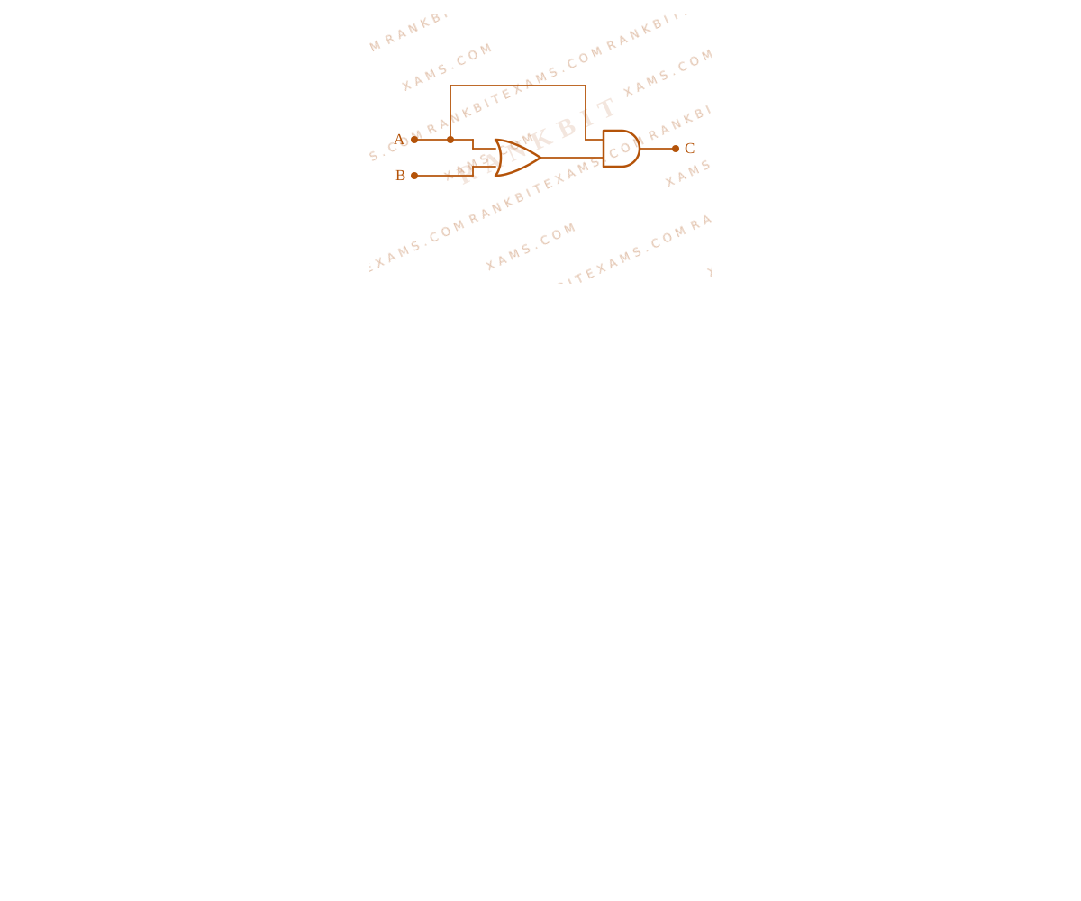
The truth table corresponding to the circuit given below is: Diagram showing a combination of logic gates connected to inputs A and B resulting in output C.
A.Table 1$\text{Table 1}$
B.Table 2$\text{Table 2}$
C.Table 3$\text{Table 3}$
D.Table 4$\text{Table 4}$
Solution
Related Formula
Boolean operators for basic logic gates:
OR gate:
Y = A + B$Y = A + B$
AND gate:
Y = A · B$Y = A \cdot B$
Core Logic
Analyze the schematic:
Input lines A$A$ and B$B$ are linked into an OR gate, yielding output:
Y = A + B$Y = A + B$
This term A + B$A + B$ and the original input line A$A$ form the inputs to a final AND gate.
The final output expression C$C$ is therefore:
C = A · (A + B)$$C = A \cdot (A + B)$$
Diagram showing a combination of logic gates connected to inputs A and B resulting in output C.
C = A · (A + B) = A · A + A · B = A + A · B$$C = A \cdot (A + B) = A \cdot A + A \cdot B = A + A \cdot B$$
By absorption law:
A + A · B = A$$A + A \cdot B = A$$
So the circuit is equivalent to a simple buffer carrying input A$A$. The output C$C$ must match input A$A$ under all conditions. Checking the options, Table 2 is the one where output C$C$ tracks input A$A$ directly (0, 1, 0, 1$0, 1, 0, 1$).
Chapter Mix
Class 12 Physics: Semiconductors
Qjee_main_2025_07_april_morningZener Diode
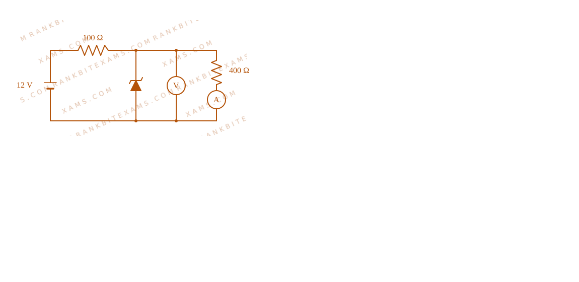
In the following circuit, the reading of the ammeter will be (Take Zener breakdown voltage = 4 V) A schematic showing a 12V supply connected to a series 100 ohm resistor, which then branches into a parallel Zener diode and a 400 ohm resistor in series with an ammeter.
A schematic showing a 12V supply connected to a series 100 ohm resistor, which then branches into a parallel Zener diode and a 400 ohm resistor in series with an ammeter.
A.24mA$24\mathrm{mA}$
B.80mA$80\mathrm{mA}$
C.10mA$10\mathrm{mA}$
D.60mA$60\mathrm{mA}$
Solution
Related Formula
Voltage division across load RL$R_L$ with series resistance Rₛ$R_s$ without Zener regulation:
Sees: Parallel Zener diode configuration.
Shortcut: Always calculate the open-circuit load voltage first. If it exceeds Vz$V_z$, use Vz$V_z$ as the branch potential. The branch current is simply Vz / RL$V_z / R_L$. Here, 4 / 400 = 10 ~mA$4 / 400 = 10 \mathrm{~mA}$.
Chapter Mix
Class 12 Physics: Semiconductor Electronics: Materials, Devices and Simple Circuits
Q8jee_main_2025_08_april_eveningDiodes
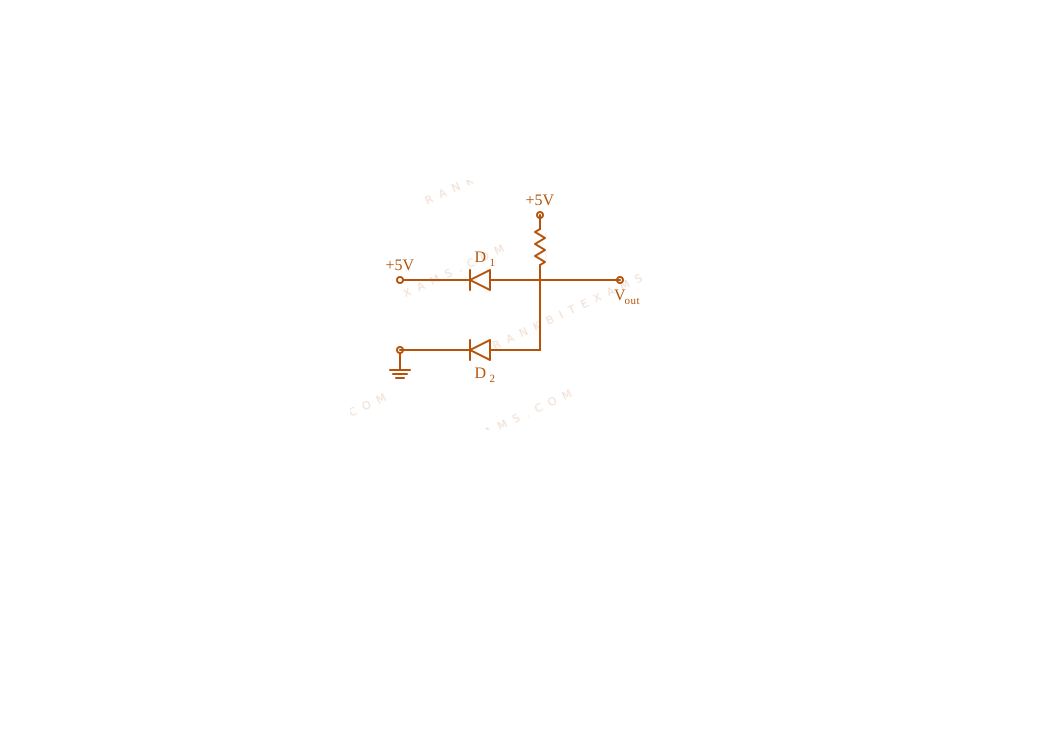
The output voltage in the following circuit is (Consider ideal diode case)
A schematic of a circuit showing an input voltage, two diodes D1 and D2 connected in parallel paths, a resistor, and the output node V_out.
A.10~V$10\mathrm{~V}$
B.0~V$0\mathrm{~V}$
C.+5~V$+5\mathrm{~V}$
D.-5~V$-5\mathrm{~V}$
Solution
Related Formula
For ideal diodes:
Forward Bias: Acts as a closed switch (zero resistance, short circuit).
Reverse Bias: Acts as an open switch (infinite resistance, open circuit).
Core Logic
Analyzing the bias condition of the diodes based on the applied potential in the schematic:
Diode D₁$D_1$ is oriented such that its cathode faces the positive terminal (+5~V$+5\mathrm{~V}$), making it Reverse Biased (no current flows through this branch).
Diode D₂$D_2$ is oriented such that its anode connects to the +5~V$+5\mathrm{~V}$ path, making it Forward Biased.
Since D₂$D_2$ is forward-biased and ideal, it acts as a short circuit (resistance RD = 0$R_D = 0$). Current flows through D₂$D_2$ and through the series resistor.
Step 1: Calculating output node potential
Because the forward-biased ideal diode D₂$D_2$ connects the node directly to the low-resistance ground loop or the reference resistor drop, the entire 5~V$5\mathrm{~V}$ potential drops across the resistor:
Vout = 0~V$$V_{\text{out}} = 0\mathrm{~V}$$
Pattern Recognition
Sees: Parallel diode configuration with opposite polarities.
Shortcut: Check polarity. D₁$D_1$ is reverse-biased (open), D₂$D_2$ is forward-biased (short). The output terminal is pulled down to the reference ground, leading directly to 0~V$0\mathrm{~V}$. ✓
Chapter Mix
Class 12 Physics: Semiconductor Electronics
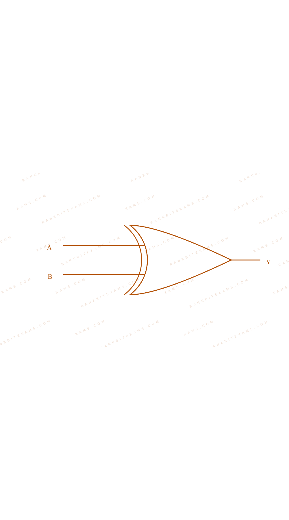
Q18jee_main_2025_29_jan_eveningLogic Gates
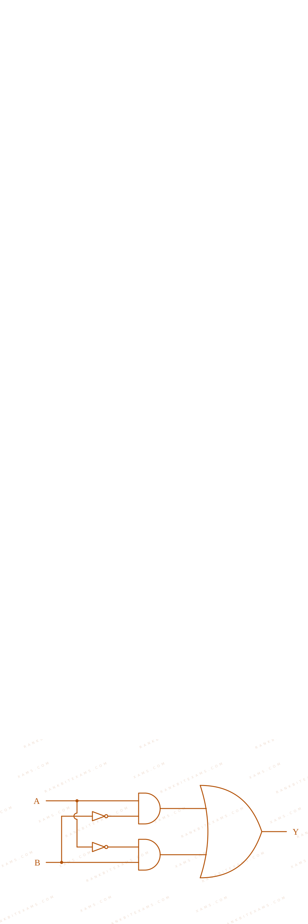
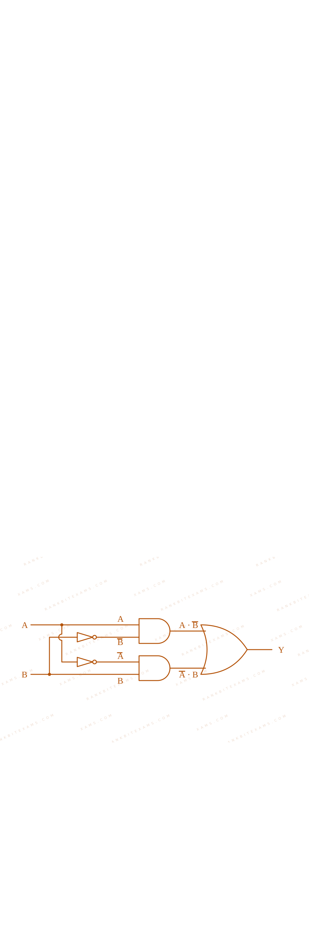
The truth table for the circuit given below is :
The image shows a digital logic circuit containing multiple interconnected logic gates with input terminals A and B and output terminal Y.
Y = A · B + A · B = A B$$Y = A \cdot \bar{B} + \bar{A} \cdot B = A \oplus B$$
Core Logic
Analyzing the circuit layout:
The top AND gate receives inputs A$A$ and B$\bar{B}$, yielding output term A B$A\bar{B}$.
The bottom AND gate receives inputs A$\bar{A}$ and B$B$, yielding output term AB$\bar{A}B$.
These terms pass into a terminal OR gate, producing:
Y = A B + AB$$Y = A\bar{B} + \bar{A}B$$
The image shows a digital logic circuit containing multiple interconnected logic gates with input terminals A and B and output terminal Y.The image shows a digital logic circuit containing multiple interconnected logic gates with input terminals A and B and output terminal Y.
This is the precise expression for an XOR (Exclusive OR) gate. The corresponding truth table gives an output of 1$1$ only when inputs are mismatched (0,1$0,1$ or 1,0$1,0$), and 0$0$ otherwise. This aligns exactly with Option 1.
Pattern Recognition
Recognize the symmetric cross-inversion network of gates: (A · B) + ( A · B)$(A \cdot \bar{B}) + (\bar{A} \cdot B)$. This combination structurally builds an XOR logic function.
Chapter Mix
Class 12 Physics: Semiconductor Electronics
More Semiconductor Electronics: Materials, Devices and Simple Circuits Questions — jee_main_2024_29_jan_morning
Practice past-year questions one chapter at a time. Pick an exam → subject → chapter and get every PYQ for that topic — pulled together from all past papers — with the chapter's key formulas alongside.