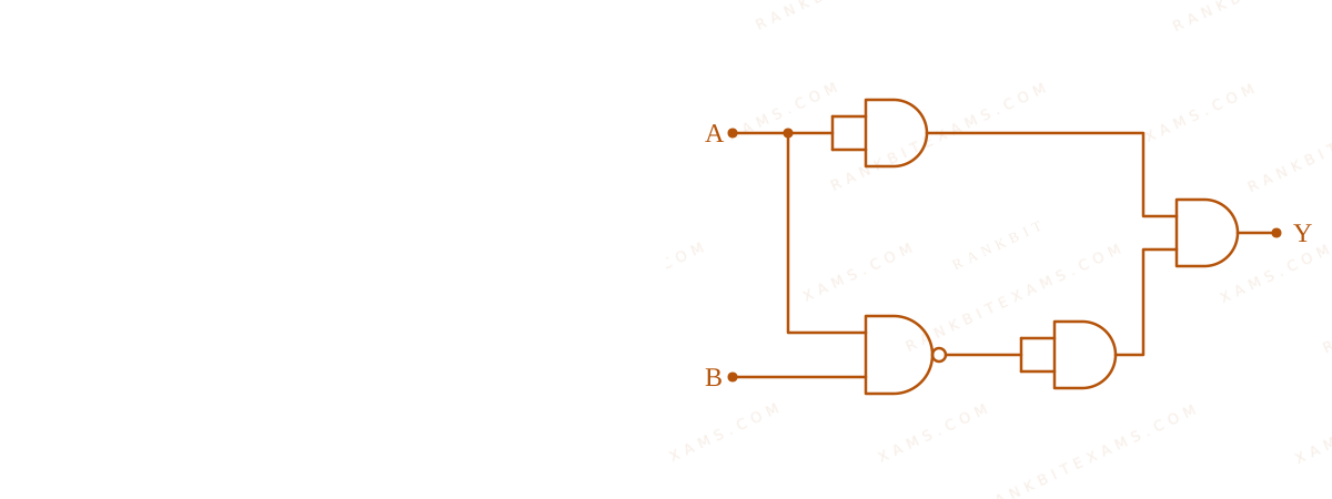
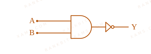
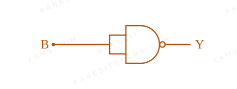
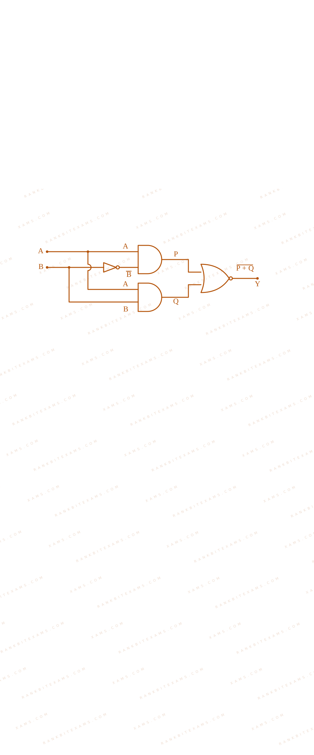
Which of the following circuits has the same output as that of the given circuit?
A combination gate circuit configuration evaluated for total Boolean output expressions.
A.
A combination gate circuit configuration evaluated for total Boolean output expressions.
B.
A combination gate circuit configuration evaluated for total Boolean output expressions.
C.
A combination gate circuit configuration evaluated for total Boolean output expressions.
D.
A combination gate circuit configuration evaluated for total Boolean output expressions.
Solution & Explanation
Core Logic
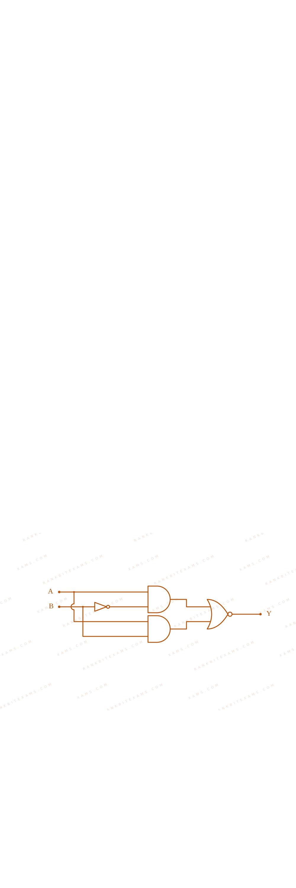
Let's perform Boolean analysis on the configuration steps mapped below:
P = A · B$$\mathrm{P} = \mathrm{A} \cdot \bar{\mathrm{B}}$$Q = A · B$$\mathrm{Q} = \mathrm{A} \cdot \mathrm{B}$$Y = P + Q = A · B + A · B$$\mathrm{Y} = \overline{\mathrm{P} + \mathrm{Q}} = \overline{\mathrm{A} \cdot \bar{\mathrm{B}} + \mathrm{A} \cdot \mathrm{B}}$$
Factoring using distributive Boolean rules:
Y = A · (B + B) = A · 1$$\mathrm{Y} = \overline{\mathrm{A} \cdot (\mathrm{B} + \bar{\mathrm{B}})} = \overline{\mathrm{A} \cdot 1}$$Y = A$$\mathrm{Y} = \bar{\mathrm{A}}$$
Step 1: Final Reduction
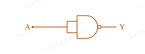
The expression reduces to a simple inverter (NOT gate) processing input A. This aligns with Circuit (1), matching option (1).
Pattern Recognition
Identify standard combinations: (A AND NOT B) OR (A AND B)$(\mathrm{A} \text{ AND NOT } \mathrm{B}) \text{ OR } (\mathrm{A} \text{ AND } \mathrm{B})$ collapses back into simply input A because operand B covers all possible states.
Chapter Mix
Class 12 Physics: Semiconductor Electronics: Materials, Devices and Simple Circuits
A combination gate circuit configuration evaluated for total Boolean output expressions.
More Semiconductor Electronics: Materials, Devices and Simple Circuits Previous-Year Questions — Page 2
Q48jee_main_2026_24_january_morningZener Diode
A voltage regulating circuit consisting of Zener diode, having break-down voltage of 10 V and maximum power dissipation of 0.4 W, is operated at 15 V. The approximate value of protective resistance in this circuit is ____ Ω$\Omega$.
Numerical Answer.Answer: 125 to 125
Solution
Related Formula
PZ = VZ IZ$P_Z = V_Z I_Z$
Vᵢₙ = IZ RS + VZ$$V_{\text{in}} = I_Z R_S + V_Z$$
Core Logic
For the Zener diode, the maximum power dissipated is:
PD = 0.4 W$$P_D = 0.4 \text{ W}$$
Since PD = VZ IZ$P_D = V_Z I_Z$:
0.4 = 10 × IZ IZ = 0.04 A$$0.4 = 10 \times I_Z \implies I_Z = 0.04 \text{ A}$$
Step 1: Find Protective Series Resistance
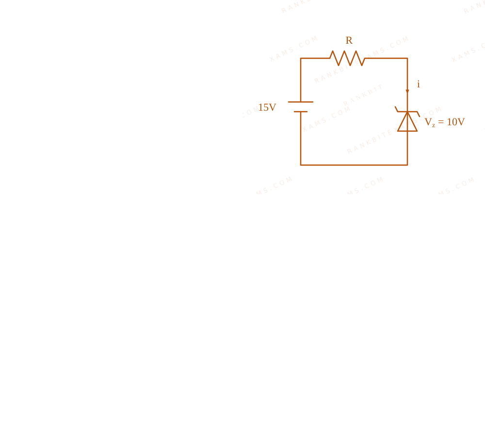
Zener diode voltage regulator circuit
The voltage drop across the series protective resistance R$R$ is:
To secure a Zener against burning out, calculate its max safe current via Pmax / Vz$P_{max} / V_z$. Feed this current into the required voltage drop (Vᵢₙ - Vz$V_{in} - V_z$) to get the exact protective resistance.
De Morgan's Laws: A · B = A + B$$\text{De Morgan's Laws: } \overline{A \cdot B} = \overline{A} + \overline{B}$$
Core Logic
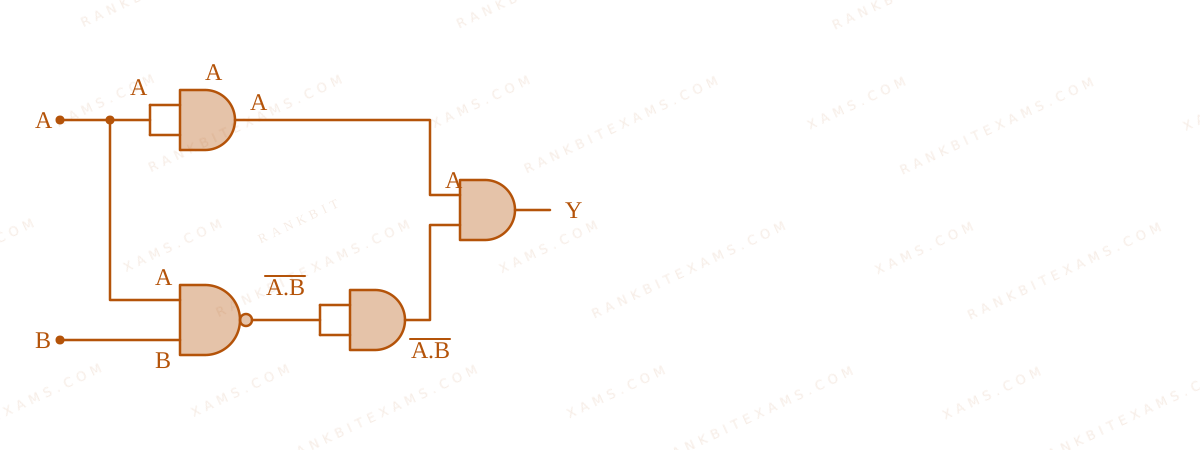
A combination of logic gates resulting in output Y.
Let's trace the logic line by line.
Top branch: A passes through an AND gate with both inputs tied to A, so it remains A$A$.
Bottom branch: A and B pass through a NAND gate, yielding A · B$\overline{A \cdot B}$. Then it passes through an AND gate with inputs tied together, so it remains A · B$\overline{A \cdot B}$.
Step 1: Boolean Expression
Finally, the inputs A$A$ and A · B$\overline{A \cdot B}$ are fed into a final AND gate.
Y = A · A · B$$Y = A \cdot \overline{A \cdot B}$$
Applying De Morgan's Law:
Y = A · ( A + B)$$Y = A \cdot (\overline{A} + \overline{B})$$Y = A · A + A · B$$Y = A \cdot \overline{A} + A \cdot \overline{B}$$
Step 2: Simplify
Since A · A = 0$A \cdot \overline{A} = 0$, we have:
Y = 0 + A B = A B$$Y = 0 + A \overline{B} = A \overline{B}$$
Checking values:
If A=1, B=0$A=1, B=0$, then Y = 1 · 1 = 1$Y = 1 \cdot 1 = 1$.
For all other combinations, Y = 0$Y = 0$.
A combination of logic gates resulting in output Y.
Pattern Recognition
An AND gate acting on A$A$ and NAND(A, B)$\text{NAND}(A, B)$ inherently acts as a "strictly A and NOT B" checker. The boolean algebra instantly simplifies A( AB)$A(\overline{AB})$ to A B$A\overline{B}$.
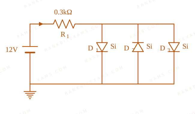
Assuming in forward bias condition there is a voltage drop of 0.7 V across a silicon diode, the current through diode D₁$D_{1}$ in the circuit is ____ mA. (Assume all diodes in the given circuit are identical)
Circuit containing a 12V source, a 0.3kOhm resistor, and three diodes D1, D2, D3 in parallel.
A.20.15$20.15$
B.11.7$11.7$
C.17.6$17.6$
D.18.8$18.8$
Solution
Related Formula
I = (V - Vd)/(R)$$I = \frac{V - V_d}{R}$$
Core Logic
Check the polarity of the battery to determine which diodes are forward-biased. Diodes D₁$D_1$ and D₂$D_2$ are forward-biased, while D₃$D_3$ is reverse-biased (acts as an open circuit). Because D₁$D_1$ and D₂$D_2$ are in parallel, the total voltage drop across the parallel combination is just 0.7 ~V$0.7 \mathrm{~V}$.
Step 1: Loop Equation
Applying KVL to the main loop containing the forward-biased diodes:
Rounding to nearest option gives 18.8 ~mA$18.8 \mathrm{~mA}$.
Pattern Recognition
Identical diodes in parallel share the current equally. The voltage drop across the entire parallel diode bank is just the drop of one diode (0.7 ~V$0.7 \mathrm{~V}$).
Chapter Mix
Class 12 Physics: Semiconductor Electronics: Materials, Devices and Simple Circuits
Q30jee_main_2026_28_january_eveningLogic Gates
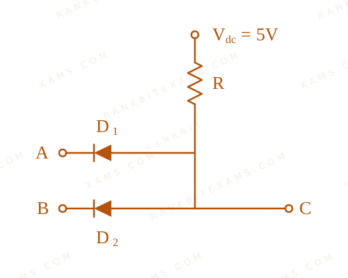
Two p-n junction diodesD₁$D_{1}$ and D₂$D_{2}$ are connected as shown in figure. A logic gate formed using two diodes connected to a 5V supply through a pull-up resistor. A and B are input signals and C is the output. The given circuit will function as a ____.
A.OR Gate$\text{OR Gate}$
B.NOR Gate$\text{NOR Gate}$
C.NAND Gate$\text{NAND Gate}$
D.AND Gate$\text{AND Gate}$
Solution
Core Logic
The circuit contains two diodes with their n-sides connected to the inputs A and B, and their p-sides tied together and connected to +5V$+5\text{V}$ through a resistor R$R$. The output C is taken from the common p-side junction.
Step 1: Analyzing the Truth Table
If either A = 0$A = 0$ (ground) or B = 0$B = 0$ (ground), the corresponding diode becomes forward biased. Current flows through the resistor R$R$, dropping the voltage at C to near 0V$0\text{V}$ (Logic 0).
If both A = 1$A = 1$ (+5V$+5\text{V}$) and B = 1$B = 1$ (+5V$+5\text{V}$), both diodes are reverse biased. No current flows through R$R$, so the voltage at C remains at +5V$+5\text{V}$ (Logic 1).
Step 2: Conclusion
The output C is 1 ONLY when both inputs A AND B are 1.
This corresponds exactly to the truth table of an AND Gate.
Pattern Recognition
Diodes pointing away from the inputs with a pull-up resistor (connected to +Vcc$+V_{cc}$) form an AND gate. If diodes point towards the inputs with a pull-down resistor to ground, it's an OR gate.
Chapter Mix
Class 12 Physics: Semiconductor Electronics: Materials, Devices and Simple Circuits
Q13jee_main_2025_02_april_eveningLogic Gates
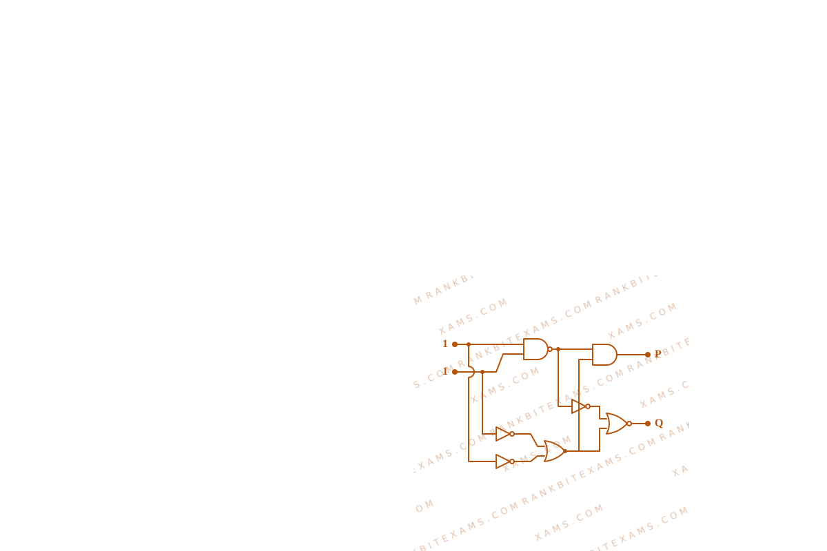
In the digital circuit shown in the figure, for the given inputs the P and Q values are :
The circuit has two inputs equal to 1, passing through multiple gates to produce outputs P and Q.
A.P = 1, Q = 1$\mathrm{P} = 1, \mathrm{Q} = 1$
B.P = 0, Q = 0$\mathrm{P} = 0, \mathrm{Q} = 0$
C.P = 0, Q = 1$\mathrm{P} = 0, \mathrm{Q} = 1$
D.P = 1, Q = 0$\mathrm{P} = 1, \mathrm{Q} = 0$
Solution
Related Formula
Truth relations of basic logic operations:
NAND operation: Y = A · B$Y = \overline{A \cdot B}$
NOR operation: Y = A + B$Y = \overline{A + B}$
NOT operation: Y = A$Y = \overline{A}$
OR operation: Y = A + B$Y = A + B$
Core Logic
The inputs are:
Top input = 1$1$
Bottom input = 1$1$
Let's analyze step-by-step from left to right:
First Gate (NAND gate at the top-left):
Inputs are 1$1$ and 1$1$.
Output = 1 · 1 = 0$\overline{1 \cdot 1} = 0$.
Bottom-left path with NOT gates:
Top input (1$1$) goes to a NOT gate, producing 0$0$.
Bottom input (1$1$) goes to a NOT gate, producing 0$0$.
These two 0$0$ values feed into the OR gate:
Output = 0 + 0 = 0$0 + 0 = 0$.
Step 1: Calculate output P
Now trace the path to P$P$:
The inputs to the top-right AND gate are:
Output of the top-left NAND gate = 0$0$
Output of the bottom-left OR gate = 0$0$
Therefore, output P$P$ is:
P = 0 · 0 = 0$$P = 0 \cdot 0 = 0$$
Step 2: Calculate output Q
Now trace the path to Q$Q$:
The gate at the bottom-right is a NOR gate with two inputs:
Input 1: Output of the top-left NAND gate (0$0$) inverted by a NOT gate = 0 = 1$\overline{0} = 1$.
Input 2: Output of the bottom-left OR gate (0$0$).
Passing these inputs (1$1$ and 0$0$) through the final NOR gate:
Sees: Combinational trace with inverted nodes.
Trap: Missing bubbles (NOT gates) representing inversion on internal circuit paths.
Shortcut: The first NAND gate output is 0$0$ (since both inputs are 1). This 0$0$ directly goes to the upper AND gate, immediately guaranteeing output P = 0$P = 0$ (eliminates options 1 and 4). Now, you only need to evaluate Q$Q$ to choose between options 2 and 3.
Chapter Mix
Class 12 Physics: Semiconductor Electronics: Materials, Devices and Simple Circuits
More Semiconductor Electronics: Materials, Devices and Simple Circuits Questions — jee_main_2025_28_jan_morning
Practice past-year questions one chapter at a time. Pick an exam → subject → chapter and get every PYQ for that topic — pulled together from all past papers — with the chapter's key formulas alongside.