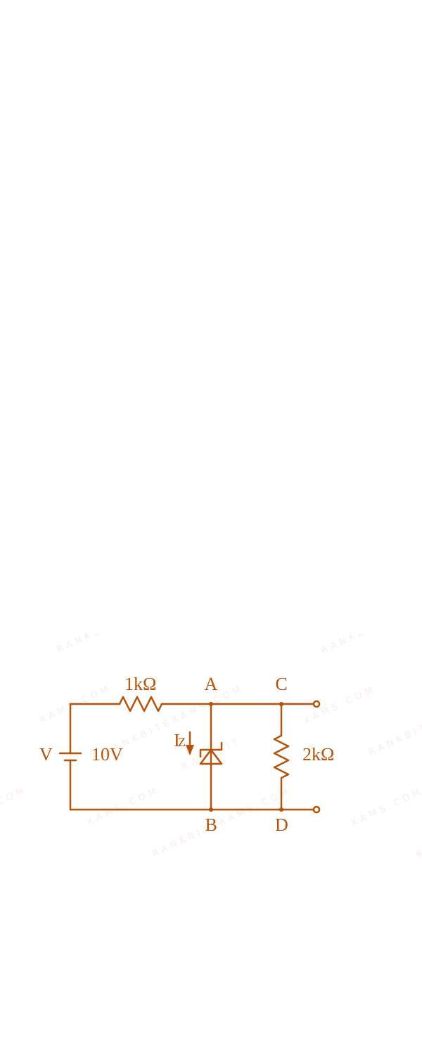
In the given circuit, the breakdown voltage of the Zener diode is 3.0 ~V$3.0 \mathrm{~V}$. What is the value of Iz$I_{z}$?
The image shows a circuit diagram with a 10V DC source connected in series with a 1kΩ resistor, followed by a parallel combination of a Zener diode (with current Iz) and a 2kΩ load resistor.
The image shows a circuit diagram with a 10V DC source connected in series with a 1kΩ resistor, followed by a parallel combination of a Zener diode (with current Iz) and a 2kΩ load resistor.
A.3.3 ~mA$3.3 \mathrm{~mA}$
B.5.5 ~mA$5.5 \mathrm{~mA}$
C.10 ~mA$10 \mathrm{~mA}$
D.7 ~mA$7 \mathrm{~mA}$
Solution & Explanation
Related Formula
For a parallel circuit regulator using a Zener diode:
I = Iz + I₁$I = I_z + I_1$
where,
I$I$ = total current through the series resistor
Iz$I_z$ = current through the Zener diode
I₁$I_1$ = current through the load resistor
Core Logic
Given that the breakdown voltage of the Zener diode is:
Vz = 3.0 ~V$$V_z = 3.0 \mathrm{~V}$$
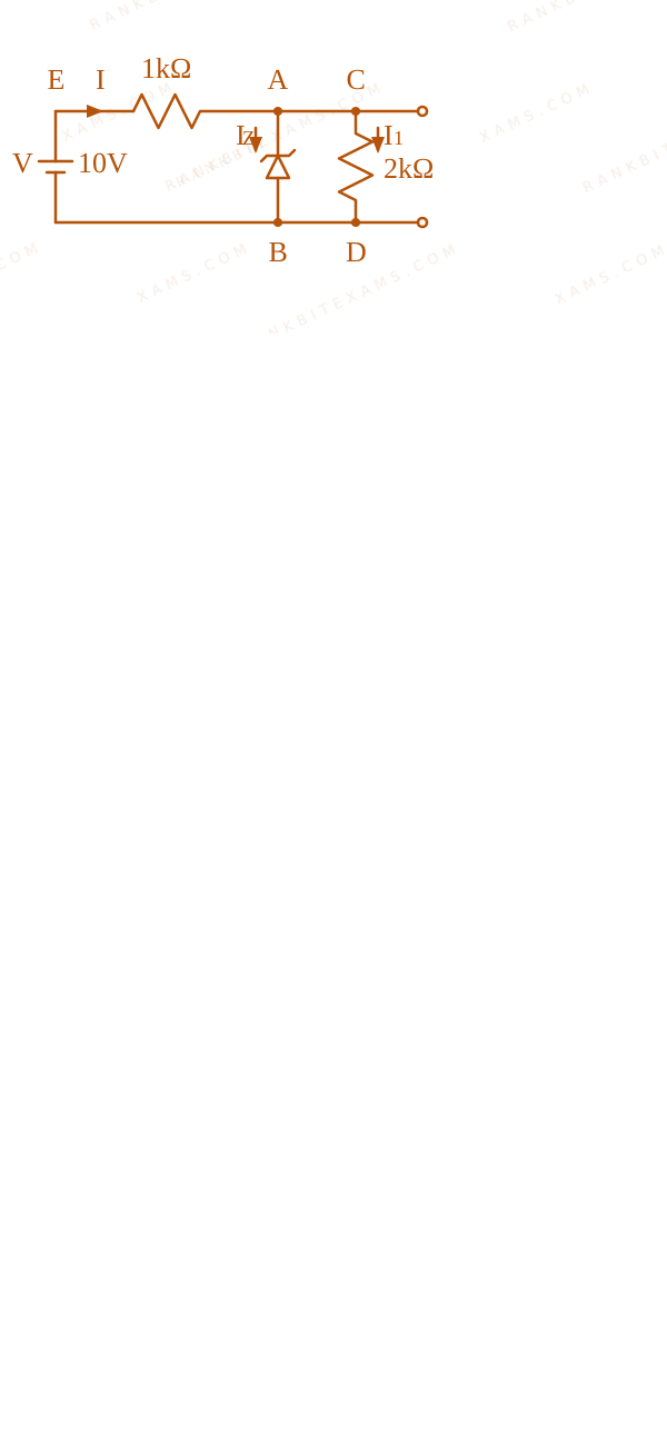
Let potential at junction B$B$ and D$D$ be 0 ~V$0 \mathrm{~V}$. Then, the potential at the Zener cathode A$A$ and load node C$C$ is stabilized at:
VA = VC = 3.0 ~V$$V_A = V_C = 3.0 \mathrm{~V}$$
Potential at the source input E$E$ is 10 ~V$10 \mathrm{~V}$.
Step 1: Calculate Total Current
The potential drop across the series resistor (1 ~kΩ$1 \mathrm{~k}\Omega$) is:
The image shows a circuit diagram with a 10V DC source connected in series with a 1kΩ resistor, followed by a parallel combination of a Zener diode (with current Iz) and a 2kΩ load resistor.
Step 2: Calculate Load Current
The voltage across the load resistor (2 ~kΩ$2 \mathrm{~k}\Omega$) is equal to Vz = 3 ~V$V_z = 3 \mathrm{~V}$. Thus, the load current I₁$I_1$ is:
Iz = I - I₁ = 7 ~mA - 1.5 ~mA = 5.5 ~mA$$I_z = I - I_1 = 7 \mathrm{~mA} - 1.5 \mathrm{~mA} = 5.5 \mathrm{~mA}$$
Therefore, the current through the Zener diode is 5.5 ~mA$5.5 \mathrm{~mA}$.
Pattern Recognition
Whenever you see a Zener diode in breakdown connected parallel to a load, always fix the node potential at the breakdown voltage. Work backwards from the supply potential to find the total current, calculate the load current using Ohm's law, and subtract to find the Zener current.
Chapter Mix
Class 12 Physics: Semiconductor Electronics: Materials, Devices and Simple Circuits
Keywords:#Zener diode#Regulator circuit#Breakdown voltage
More Semiconductor Electronics: Materials, Devices and Simple Circuits Previous-Year Questions — Page 7
Q49jee_main_2024_31_jan_eveningLogic Gates
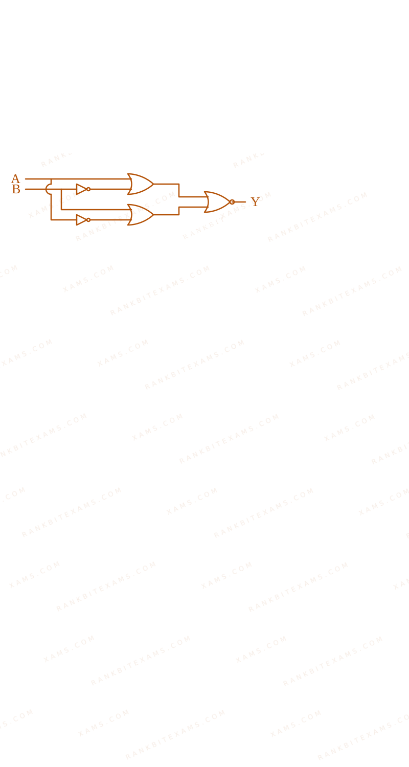
The output of the given circuit diagram is
The image shows a logic circuit composed of NOT gates, OR gates, and a final NOR gate.
A.
A
B
Y
0
0
0
1
0
0
0
1
0
1
1
1
B.
A
B
Y
0
0
0
1
0
1
0
1
1
1
1
0
C.
A
B
Y
0
0
0
1
0
0
0
1
0
1
1
0
D.
A
B
Y
0
0
0
1
0
0
0
1
1
1
1
0
Solution
Related Formula
Boolean Algebra expressions for logic gates:
NOT: A$\overline{A}$
OR: A + B$A + B$
NOR: A + B$\overline{A + B}$
Core Logic
Analyze the paths from inputs A and B to the final output Y.
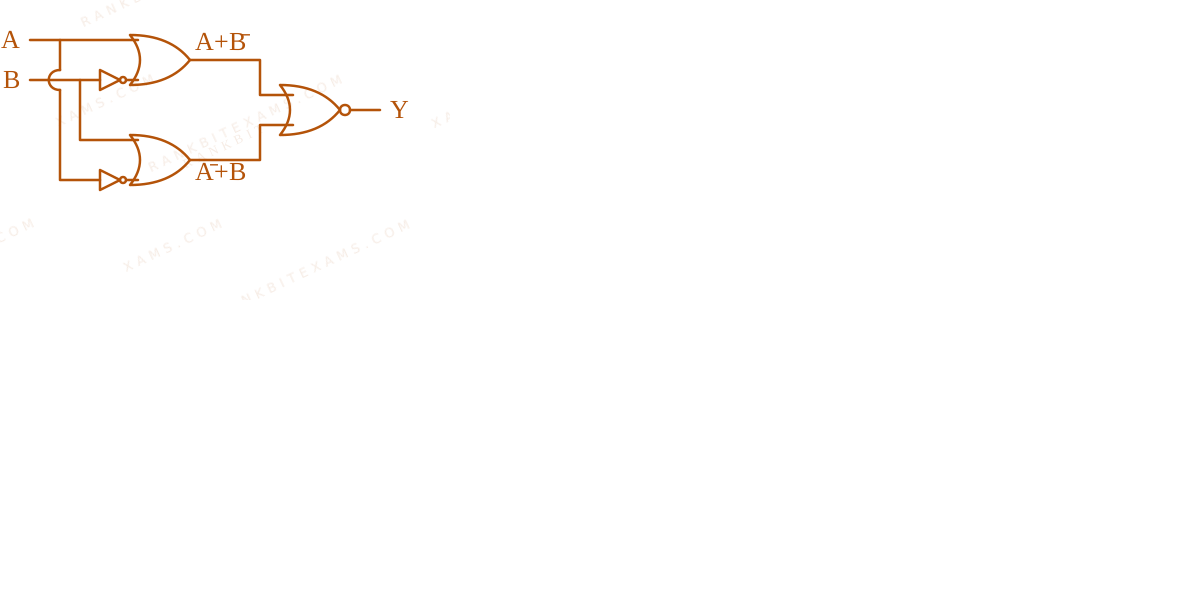
The image shows a logic circuit composed of NOT gates, OR gates, and a final NOR gate.
Step 1: Intermediate Signals
Top OR gate inputs: A$A$ directly, and B$B$ inverted (B$\overline{B}$).
Top OR gate output: A + B$A + \overline{B}$
Bottom OR gate inputs: A$A$ inverted (A$\overline{A}$), and B$B$ directly.
Bottom OR gate output: A + B$\overline{A} + B$
Step 2: Final Gate Evaluation
The final gate is a NOR gate taking the two intermediate outputs as its inputs.
Y = (A + B) + ( A + B)$$Y = \overline{(A + \overline{B}) + (\overline{A} + B)}$$
Notice that the inner sum simplifies cleanly:
(A + A) + (B + B)$$(A + \overline{A}) + (B + \overline{B})$$
Since A + A = 1$A + \overline{A} = 1$ and B + B = 1$B + \overline{B} = 1$, the inner term is 1 + 1 = 1$1 + 1 = 1$.
Y = 1 = 0$$Y = \overline{1} = 0$$
Step 3: Conclusion
The output Y is always 0 regardless of the inputs A and B. Checking the truth tables, only option 3 satisfies Y=0$Y=0$ for all conditions.
Pattern Recognition
When a Boolean expression groups a variable and its exact complement together in an OR configuration (A$A$ and A$\overline{A}$), the result instantly hits logic 1. Feeding 1 into any NOR gate guarantees a 0 output universally.
Chapter Mix
Class 12 Physics: Semiconductor Electronics
Qjee_main_2024_31_jan_morningLogic Gates
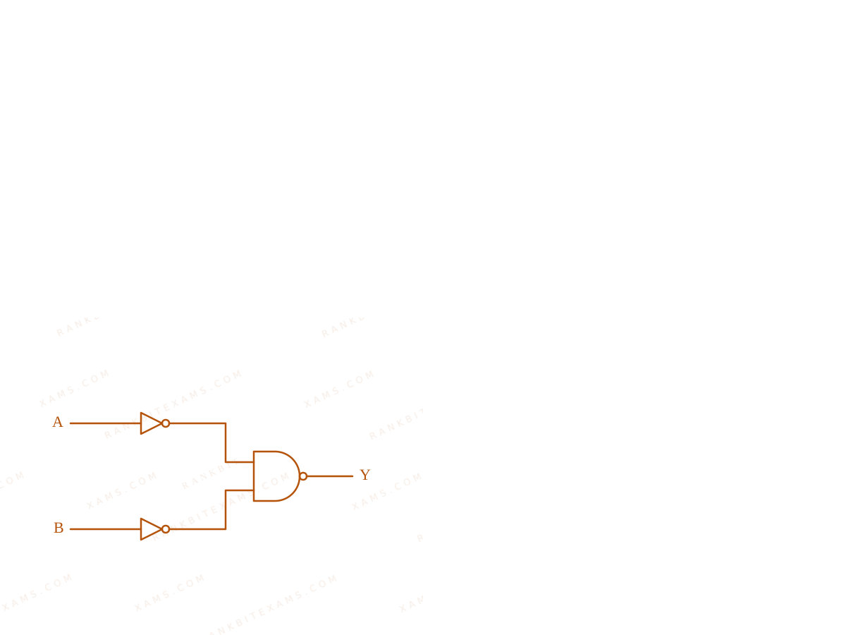
Identify the logic operation performed by the given circuit.
Two inputs passing through NOT gates before entering a NAND gate.
A.NAND$\text{NAND}$
B.NOR$\text{NOR}$
C.OR$\text{OR}$
D.AND$\text{AND}$
Solution
Related Formula
Y = A · B (NAND)$$Y = \overline{A \cdot B} \quad \text{(NAND)}$$Y = A + B (De Morgan's)$$Y = \overline{A} + \overline{B} \quad \text{(De Morgan's)}$$
Core Logic
The inputs A$A$ and B$B$ are first passed through individual NOT gates (made from tied-input NAND gates or standard NOT gates). The outputs become A$\overline{A}$ and B$\overline{B}$.
These are then fed into a NAND gate.
The final output Y$Y$ is:
Y = A · B$$Y = \overline{\overline{A} \cdot \overline{B}}$$
Applying De-Morgan's Law:
Y = A + B$$Y = \overline{\overline{A}} + \overline{\overline{B}}$$
Y = A + B$Y = A + B$
This represents an OR operation.
Pattern Recognition
Bubbled inputs on a NAND gate convert it directly into an OR gate via De-Morgan's laws. (Bubbled NAND = OR).
Chapter Mix
Class 12 Physics: Semiconductor Electronics
More Semiconductor Electronics: Materials, Devices and Simple Circuits Questions — jee_main_2024_29_jan_morning
Practice past-year questions one chapter at a time. Pick an exam → subject → chapter and get every PYQ for that topic — pulled together from all past papers — with the chapter's key formulas alongside.