Logic Gates diagram for Q15 - JEE Main 2025 Morning
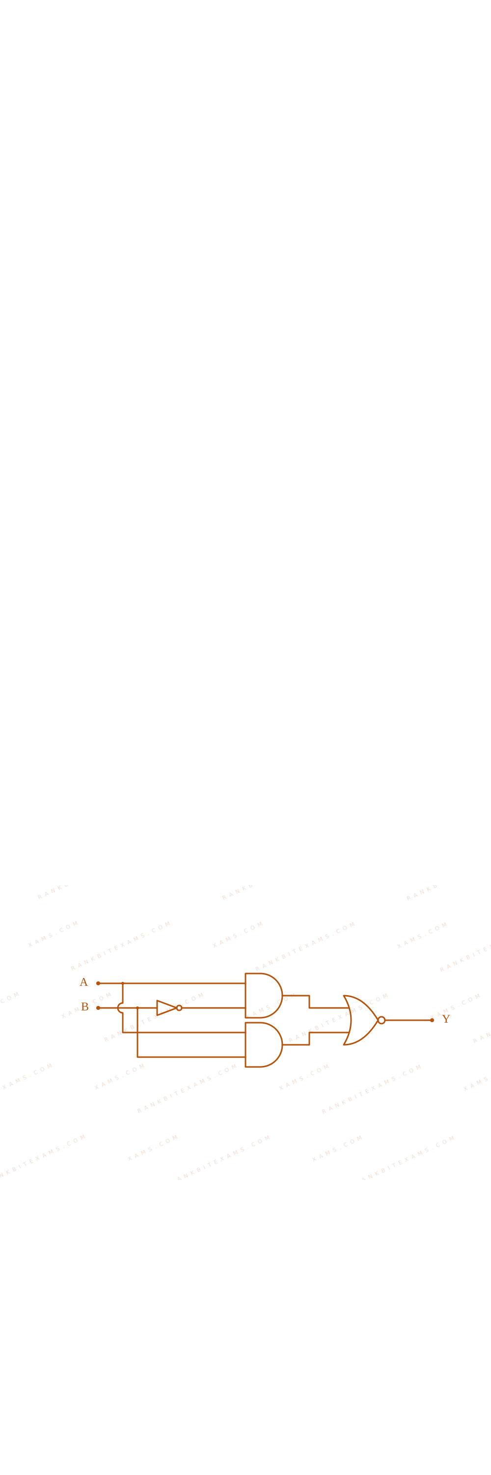
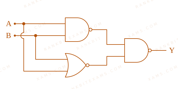
The image features a digital circuit blueprint constructed from basic logic gates with inputs A and B mapped to an output Y.
For the circuit shown above, equivalent GATE is :

Logic Gates diagram for Q15 - JEE Main 2025 Morning
The image features a digital circuit blueprint constructed from basic logic gates with inputs A and B mapped to an output Y.

Solution & Explanation

Core Logic

Evaluating the given logic gate diagram combination step-by-step for all input permutations yields the following truth table :

Input AInput BOutput Y
000
011
101
111

This behavior matches an OR Gate configuration perfectly.

Chapter Mix

Class 12 Physics: Semiconductor Electronics

More Semiconductor Electronics Previous-Year Questions — Page 4

Q jee_main_2025_28_jan_morning Logic Gates
Which of the following circuits has the same output as that of the given circuit?
Logic Gates diagram for Q13 - JEE Main 2025 Morning
A combination gate circuit configuration evaluated for total Boolean output expressions.
  • A.
  • B.
  • C.
  • D.

Solution

Core Logic

Let's perform Boolean analysis on the configuration steps mapped below:

P = A · B Q = A · B Y = P + Q = A · B + A · B

Factoring using distributive Boolean rules:

Y = A · (B + B) = A · 1 Y = A
Step 1: Final Reduction

The expression reduces to a simple inverter (NOT gate) processing input A. This aligns with Circuit (1), matching option (1).

Pattern Recognition

Identify standard combinations: (A AND NOT B) OR (A AND B) collapses back into simply input A because operand B covers all possible states.

Chapter Mix

Class 12 Physics: Semiconductor Electronics: Materials, Devices and Simple Circuits
Q jee_main_2025_03_april_morning Logic Gates
Choose the correct logic circuit for the given truth table having inputs A and B.
InputsOutput
ABY
000
010
101
111
  • A.
  • B.
  • C.
  • D.

Solution

Related Formula

Let us inspect the Boolean expression for the output Y from the truth table. From the table:

  • If A=0, Y=0 regardless of B.
  • If A=1, Y=1 regardless of B.
  • Thus, the truth table is represented by the simple direct logical equation: Y = A

Core Logic

Let's check the Boolean output of the options shown in the question paper:

  • Circuit (1): Inputs A and B go into an OR gate, outputting (A + B). This output and B then go to an AND gate.
Y = (A + B) · B = A· B + B· B = B(A + 1) = B

This gives Y = B (Not matching table).

  • Circuit (2): Inputs A and B go into an OR gate, outputting (A + B). This and A then go into an AND gate.
Y = (A + B) · A = A· A + A· B = A + A· B = A(1 + B) = A

This gives Y = A (Perfect match to the truth table where Y exactly copies A).

Step 1: Verification of Circuit (2)

Let's double-check the truth table values for Circuit (2):

  • For A=0, B=0: Y = (0 + 0) · 0 = 0.
  • For A=0, B=1: Y = (0 + 1) · 0 = 0.
  • For A=1, B=0: Y = (1 + 0) · 1 = 1.
  • For A=1, B=1: Y = (1 + 1) · 1 = 1.
  • This perfectly matches the given truth table. Therefore, Circuit (2) is correct.

Pattern Recognition

Identify the logic expression directly from the truth table first! Notice that Y is completely independent of B and strictly equals A. This immediately points to any Boolean simplification that collapses to A (such as absorption law: A(A+B) = A).

Chapter Mix

Class 12 Physics: Semiconductor Electronics: Materials, Devices and Simple Circuits

Q16 jee_main_2025_04_april_evening Extrinsic Semiconductors
Consider a n-type semiconductor in which nₑ and nh are number of electrons and holes, respectively. (A) Holes are minority carriers (B) The dopant is a pentavalent atom (C) nₑnh≠ nᵢ² (where nᵢ is number of electrons or holes in semiconductor when it is in intrinsic form) (D) nₑnh≥ nᵢ² (E) The holes are not generated due to the donors Choose the correct answer from the options given below:
  • A. (A), (C), (D) only
  • B. (A), (C), (E) only
  • C. (A), (B), (E) only
  • D. (A), (B), (C) only

Solution

Related Formula

Mass Action Law:

nₑ · nh = nᵢ²
Core Logic

Let's analyze each statement for an n-type semiconductor:

  • (A) Holes are minority carriers: True, electrons are the majority carriers.
  • (B) The dopant is a pentavalent atom: True (like Phosphorus, Arsenic) which provides extra free electrons.
  • (C) and (D) contradict the fundamental mass action law nₑ nh = nᵢ², so they are False.
  • (E) Holes are generated purely due to thermal excitation, not due to donor atoms: True.
Step 1: Assemble Correct Set

Statements (A), (B), and (E) are explicitly correct.

Pattern Recognition

Mass action law (nₑ nh = nᵢ²) holds uniformly for both doped types at thermal equilibrium. In n-type systems, donors directly inject electrons only; holes emerge solely from thermal breakages of lattice bonds.

Chapter Mix

Class 12 Physics: Semiconductor Electronics

Q jee_main_2025_04_april_morning Logic Gates
The Boolean expression Y=AoverlineBC+overlineAoverlineC can be realised with which of the following gate configurations. A. One 3-input AND gate, 3 NOT gates and one 2-input OR gate, One 2-input AND gate B. One 3-input AND gate, 1 NOT gate, One 2-input NOR gate and one 2-input OR gate C. 3-input OR gate, 3 NOT gates and one 2-input AND gate Choose the correct answer from the options given below
  • A. B, C Only
  • B. A, B Only
  • C. A, B, C Only
  • D. A, C Only

Solution

Related Formula

Given logical expression:

Y = A BC + A C

By De Morgan's laws:

A· C = A+C (NOR configuration)
Core Logic

Let's analyze configurations A and B:

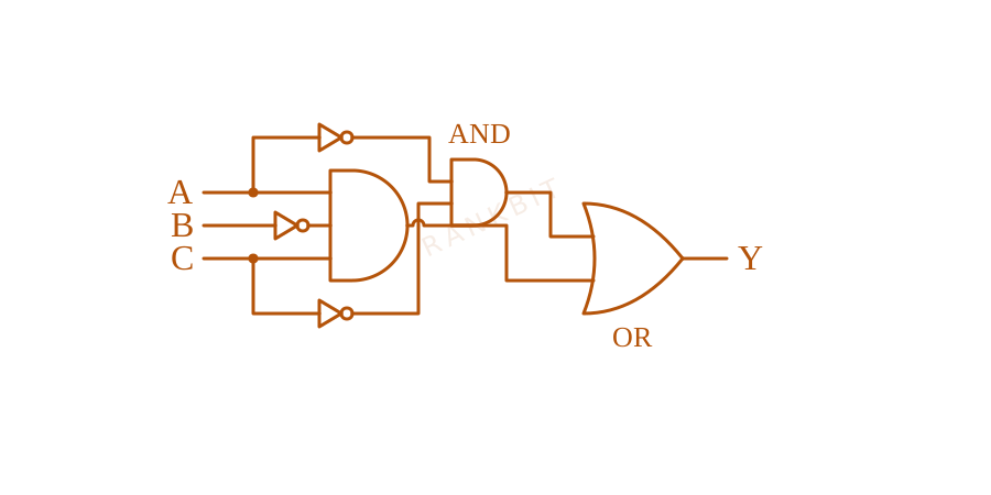
  • Configuration A: Generates A BC using one 3-input AND gate and one NOT gate for input B. Generates A C using one 2-input AND gate and two separate NOT gates for inputs A and C. Combines both terms using a 2-input OR gate.
  • (Total: one 3-input AND, one 2-input AND, three NOT gates, one 2-input OR gate).

    Logic circuit layout A for Q15 - JEE Main 2025 Morning
    Logic circuit layout A for Q15 - JEE Main 2025 Morning

Step 1: Verify Configuration B
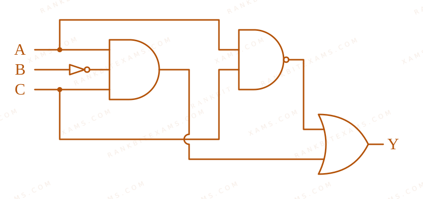
  • Configuration B: Generates A BC using one 3-input AND gate and one NOT gate for input B. Simplifies the second term A C into A+C, realized directly with a single 2-input NOR gate. Combines both sub-circuits using a 2-input OR gate.
  • (Total: one 3-input AND, one 2-input NOR, one NOT gate, one 2-input OR gate).

    Logic circuit layout A for Q15 - JEE Main 2025 Morning
    Logic circuit layout A for Q15 - JEE Main 2025 Morning

Step 2: Verify Configuration C
  • Configuration C: Specifies a 3-input OR gate and a 2-input AND gate at the output, which implements a product-of-sums form rather than the required sum-of-products expression. Hence, Configuration C is invalid.
  • Both configurations A and B correctly realize the logic function.

Pattern Recognition

Apply De Morgan's theorem (A· B = A+B) to convert negated AND products into standard NOR gate structures, reducing the total gate count.

Evaluation Rubric / Model Answer

Option B: A, B Only

Chapter Mix

Class 12 Physics: Semiconductor Electronics

Q11 jee_main_2025_07_april_evening Logic Gates
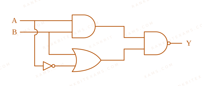
Consider the following logic circuit.
Logic Gates diagram for Q11 - JEE Main 2025 Evening
The diagram illustrates a combination of an AND gate, an inverter, an OR gate, and a terminal NAND gate with inputs A and B.
The output is Y=0 when : [cite: 64, 89]
  • A. A=1 and B=1 [cite: 90]
  • B. A=0 and B=1 [cite: 99]
  • C. A=1 and B=0 [cite: 91]
  • D. A=0 and B=0 [cite: 100]

Solution

Core Logic

Let the intermediate outputs of the first layers be Y₁ and Y₂ [cite: 747]:

  • Top gate is an AND gate with inputs A and B, so Y₁ = A · B [cite: 747].
  • Bottom gate is an OR gate where one input is B and the other is A via a NOT gate, so Y₂ = A + B [cite: 747].
  • The final layer is a NAND gate with inputs Y₁ and Y₂, so Y = Y₁ · Y₂[cite: 748].
Step 1: Constructing the Truth Table

Let's compute the output Y for all binary input pairs (A, B) [cite: 757]:

  • For A=0, B=0 Y₁ = 0, Y₂ = 1 Y = 0 · 1 = 1 [cite: 757].
  • For A=1, B=0 Y₁ = 0, Y₂ = 0 Y = 0 · 0 = 1 [cite: 757].
  • For A=0, B=1 Y₁ = 0, Y₂ = 1 Y = 0 · 1 = 1 [cite: 757].
  • For A=1, B=1 Y₁ = 1, Y₂ = 1 Y = 1 · 1 = 0 [cite: 757].
  • Thus, Y=0 uniquely when A=1 and B=1[cite: 89, 90, 757].

Pattern Recognition

A NAND gate produces an output of 0 if and only if all its inputs are 1. Working backward, this instantly sets Y₁=1 and Y₂=1. For Y₁ = A · B = 1, we must have A=1 and B=1 simultaneously.

Chapter Mix

Class 12 Physics: Semiconductors

More Semiconductor Electronics Questions — jee_main_2025_29_jan_morning

Practice all Semiconductor Electronics previous-year questions →

Rankbit System
JEE Physics: Waves (+15.5%) | Electrostatics: Concentric Shells (-29.7%) | Modern Physics: Photoelectric Clones (+34.2%) | Mathematics: Definite Integrals (+18.1%) | Chemistry: Coordination Splitting (-11.4%) | JEE Physics: Waves (+15.5%) | Electrostatics: Concentric Shells (-29.7%) | Modern Physics: Photoelectric Clones (+34.2%) | Mathematics: Definite Integrals (+18.1%) | Chemistry: Coordination Splitting (-11.4%)