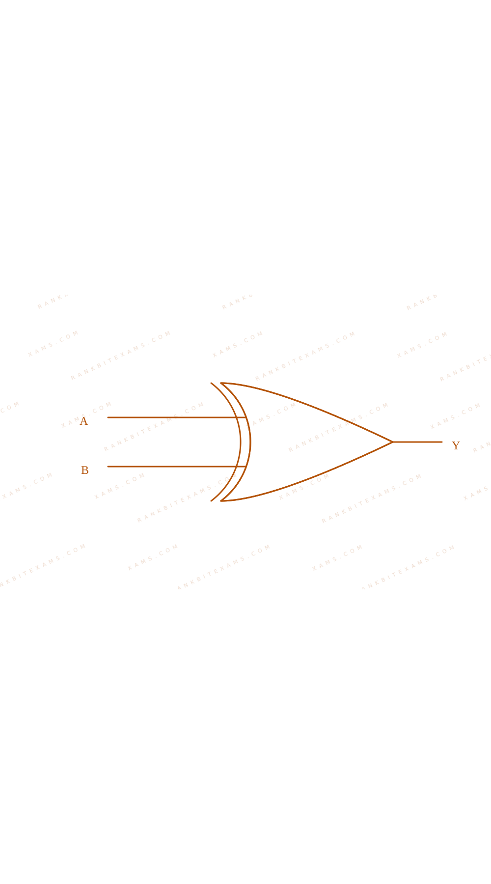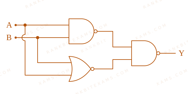
Logic Gates diagram for Q15 - JEE Main 2025 Morning
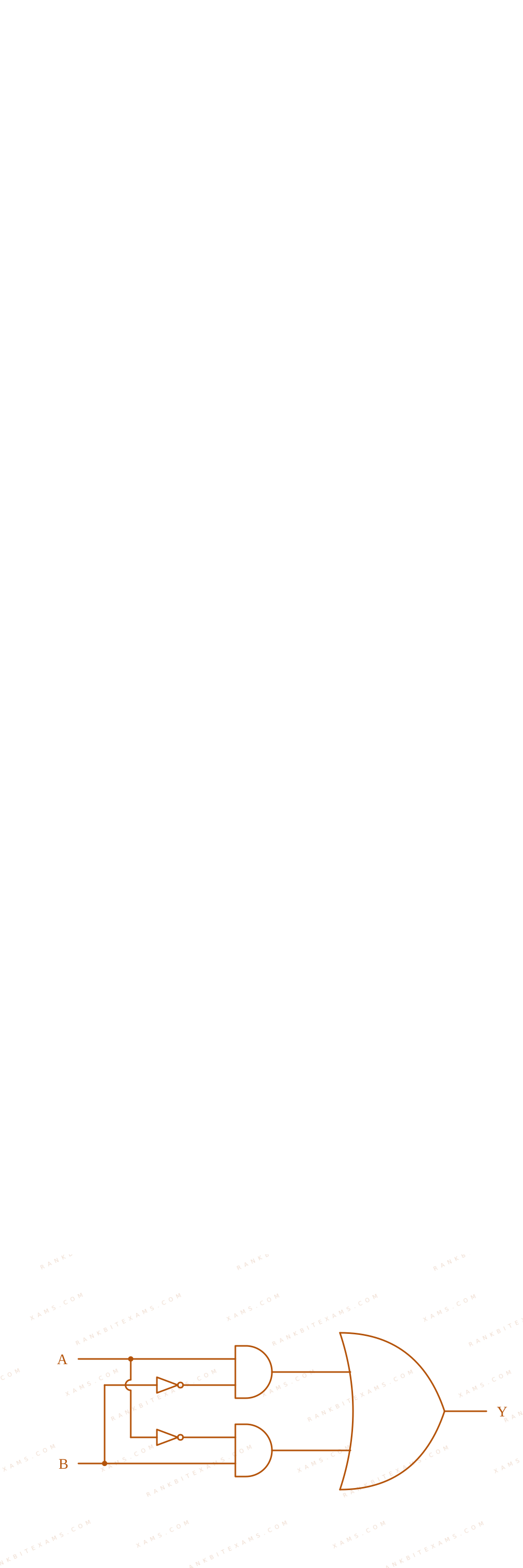
The image features a digital circuit blueprint constructed from basic logic gates with inputs A and B mapped to an output Y.
For the circuit shown above, equivalent GATE is :

Logic Gates diagram for Q15 - JEE Main 2025 Morning
The image features a digital circuit blueprint constructed from basic logic gates with inputs A and B mapped to an output Y.

Solution & Explanation

Core Logic

Evaluating the given logic gate diagram combination step-by-step for all input permutations yields the following truth table :

Input AInput BOutput Y
000
011
101
111

This behavior matches an OR Gate configuration perfectly.

Chapter Mix

Class 12 Physics: Semiconductor Electronics

More Semiconductor Electronics Previous-Year Questions — Page 3

Q11 jee_main_2025_02_april_morning Zener Diode and Voltage Regulation
A zener diode with 5~V zener voltage is used to regulate an unregulated dc voltage input of 25~V. For a 400~Ω resistor connected in series, the zener current is found to be 4 times load current. The load current (IL) and load resistance (RL) are:
  • A. IL = 20~mA; RL = 250~Ω
  • B. IL = 10~A; RL = 0.5~Ω
  • C. IL = 0.02~mA; RL = 250~Ω
  • D. IL = 10~mA; RL = 500~Ω

Solution

Related Formula
Itotal = IZ + IL Itotal = Vᵢₙ - VZRS RL = (VZ)/(IL)
Core Logic

Given parameters:

  • Input voltage, Vᵢₙ = 25~V
  • Zener breakdown voltage, VZ = 5~V
  • Series resistor, RS = 400~Ω
  • The voltage drop across the series resistor RS is:

VRS = Vᵢₙ - VZ = 25 - 5 = 20~V

The total series current I is:

Itotal = VRSRS = (20)/(400) = 0.05~A = 50~mA

We are given that the zener current IZ is 4 times the load current IL:

IZ = 4 IL

Since Itotal = IZ + IL:

50~mA = 4 IL + IL = 5 IL IL = 10~mA

The load resistance connected in parallel with the Zener diode is:

RL = (VZ)/(IL) = 5~V10 × 10⁻³~A = 500~Ω
Step 1: Final Conclusion

The load current is 10~mA and the load resistance is 500~Ω.

Pattern Recognition

In any zener regulator problem: first determine the series path current using Itotal = Vᵢₙ - VZRₛ. Split this total current using the given ratio of IZ and IL. Finally, determine RL from VZ / IL.

Chapter Mix

Class 12 Physics: Semiconductor Electronics
Q jee_main_2025_03_april_evening Logic Gates and Truth Tables
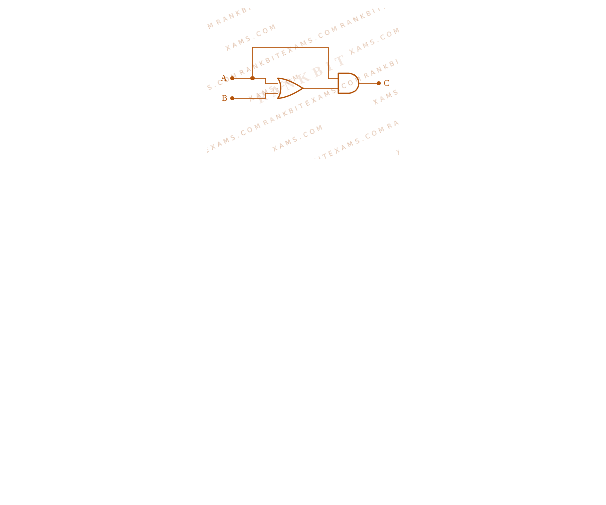
The truth table corresponding to the circuit given below is:
Logic gate circuit diagram for Q13 - JEE Main 2025 Evening
Diagram showing a combination of logic gates connected to inputs A and B resulting in output C.
  • A. Table 1
  • B. Table 2
  • C. Table 3
  • D. Table 4

Solution

Related Formula

Boolean operators for basic logic gates:

  • OR gate:
  • Y = A + B

  • AND gate:
  • Y = A · B

Core Logic

Analyze the schematic:

  • Input lines A and B are linked into an OR gate, yielding output:
  • Y = A + B

  • This term A + B and the original input line A form the inputs to a final AND gate.
  • The final output expression C is therefore:
C = A · (A + B)

Logic Gates and Truth Tables
Diagram showing a combination of logic gates connected to inputs A and B resulting in output C.

Step 1: Construct the Truth Table

Compute output values for each input combination:

  • For A=0, B=0:
C = 0 · (0 + 0) = 0
  • For A=1, B=0:
C = 1 · (1 + 0) = 1 · 1 = 1
  • For A=0, B=1:
C = 0 · (0 + 1) = 0 · 1 = 0
  • For A=1, B=1:
C = 1 · (1 + 1) = 1 · 1 = 1

This matches Table 2.

Pattern Recognition

Using Boolean algebra:

C = A · (A + B) = A · A + A · B = A + A · B

By absorption law:

A + A · B = A

So the circuit is equivalent to a simple buffer carrying input A. The output C must match input A under all conditions. Checking the options, Table 2 is the one where output C tracks input A directly (0, 1, 0, 1).

Chapter Mix

Class 12 Physics: Semiconductors

Q jee_main_2025_07_april_morning Zener Diode
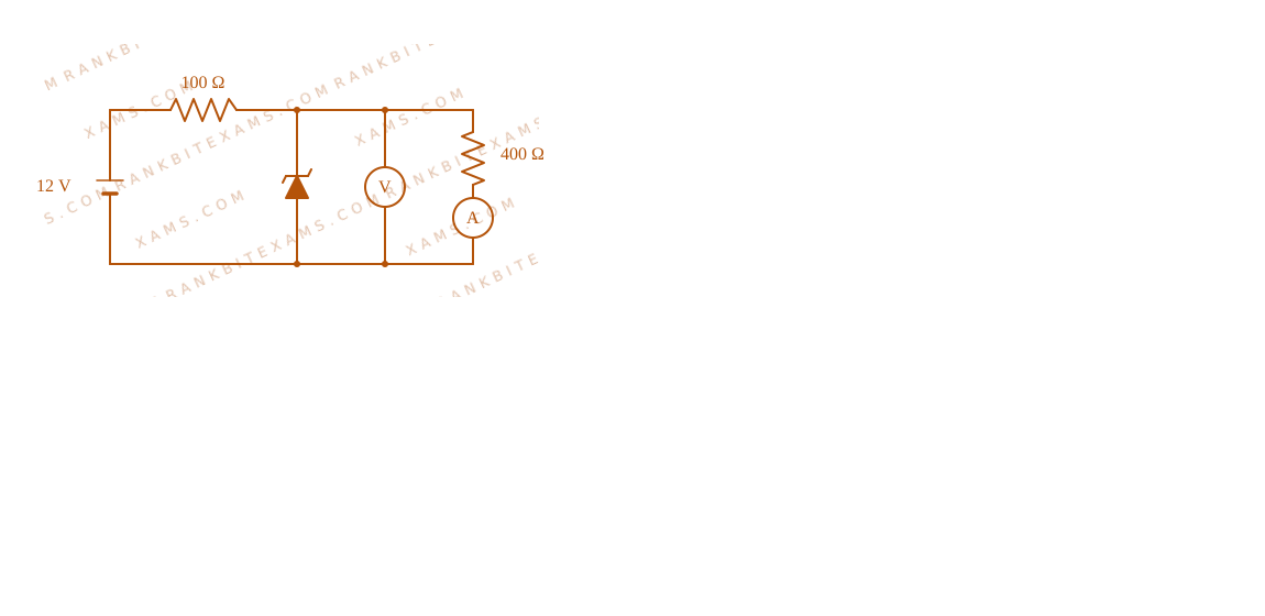
In the following circuit, the reading of the ammeter will be (Take Zener breakdown voltage = 4 V)
Zener regulator circuit for Q11 - JEE Main 2025 Morning
A schematic showing a 12V supply connected to a series 100 ohm resistor, which then branches into a parallel Zener diode and a 400 ohm resistor in series with an ammeter.
Zener regulator circuit for Q11 - JEE Main 2025 Morning
A schematic showing a 12V supply connected to a series 100 ohm resistor, which then branches into a parallel Zener diode and a 400 ohm resistor in series with an ammeter.
  • A. 24mA
  • B. 80mA
  • C. 10mA
  • D. 60mA

Solution

Related Formula

Voltage division across load RL with series resistance Rₛ without Zener regulation:

VL = Vᵢₙ ( (RL)/(Rₛ + RL) )

If VL > Vz, the Zener diode enters breakdown, and potential across the parallel load is clamped at VL = Vz.

Core Logic

Verify if Zener diode operates in the breakdown region:

  • Vᵢₙ = 12 ~V
  • Rₛ = 100 Ω
  • RL = 400 Ω
  • Calculate the unregulated voltage:

V₁ = 12 × ( (400)/(100 + 400) ) = 12 × (4)/(5) = 9.6 ~V

Since V₁ > Vz (9.6 ~V > 4 ~V), breakdown occurs, and the parallel branch voltage is fixed at Vz = 4 ~V.

Step 1: Calculate Branch Current

The voltage across the 400 Ω load resistor (which is in series with the ammeter) is locked at 4 ~V.

The current I through the ammeter is:

I = (Vz)/(RL) = 4 ~V400 Ω = 10⁻² ~A = 10 ~mA
Pattern Recognition

Sees: Parallel Zener diode configuration. Shortcut: Always calculate the open-circuit load voltage first. If it exceeds Vz, use Vz as the branch potential. The branch current is simply Vz / RL. Here, 4 / 400 = 10 ~mA.

Chapter Mix

Class 12 Physics: Semiconductor Electronics: Materials, Devices and Simple Circuits

Q8 jee_main_2025_08_april_evening Diodes
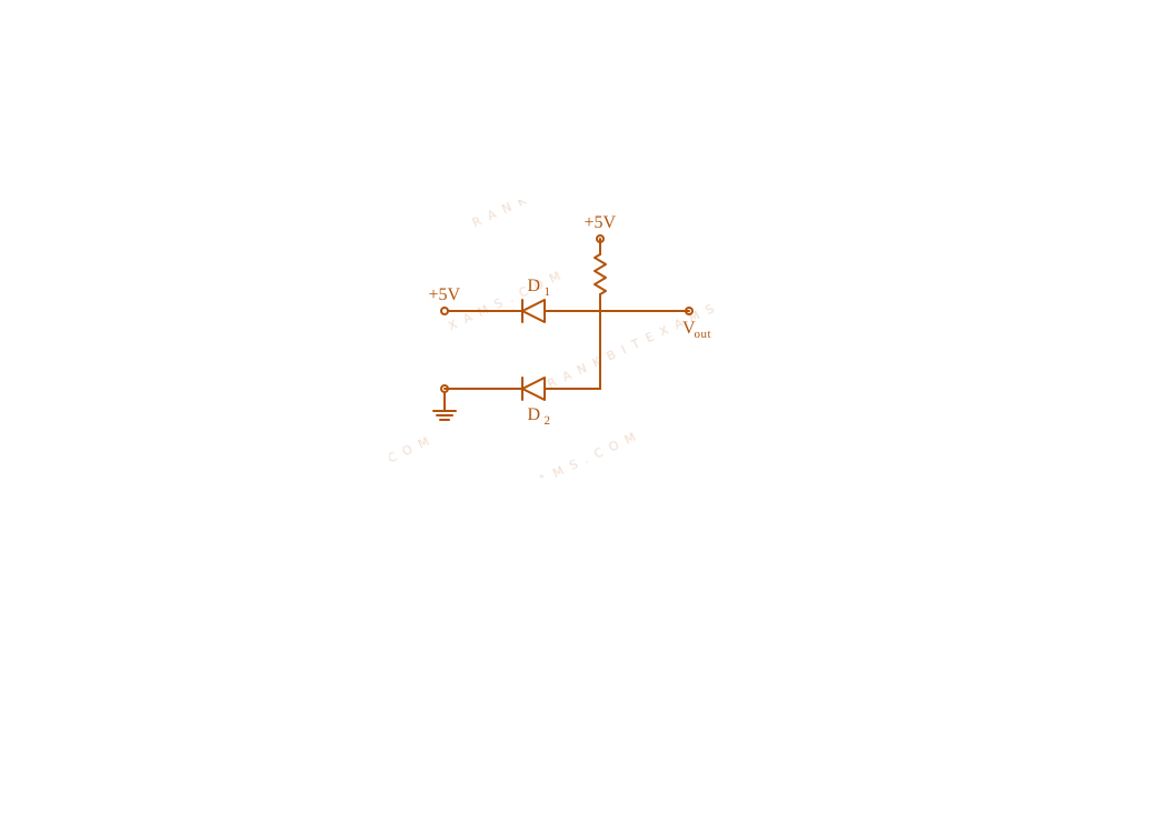
The output voltage in the following circuit is (Consider ideal diode case)
Diodes circuit diagram for Q8 - JEE Main 2025 Evening
A schematic of a circuit showing an input voltage, two diodes D1 and D2 connected in parallel paths, a resistor, and the output node V_out.
  • A. 10~V
  • B. 0~V
  • C. +5~V
  • D. -5~V

Solution

Related Formula

For ideal diodes:

  • Forward Bias: Acts as a closed switch (zero resistance, short circuit).
  • Reverse Bias: Acts as an open switch (infinite resistance, open circuit).
Core Logic

Analyzing the bias condition of the diodes based on the applied potential in the schematic:

  • Diode D₁ is oriented such that its cathode faces the positive terminal (+5~V), making it Reverse Biased (no current flows through this branch).
  • Diode D₂ is oriented such that its anode connects to the +5~V path, making it Forward Biased.
  • Since D₂ is forward-biased and ideal, it acts as a short circuit (resistance RD = 0). Current flows through D₂ and through the series resistor.

Step 1: Calculating output node potential

Because the forward-biased ideal diode D₂ connects the node directly to the low-resistance ground loop or the reference resistor drop, the entire 5~V potential drops across the resistor:

Vout = 0~V
Pattern Recognition

Sees: Parallel diode configuration with opposite polarities. Shortcut: Check polarity. D₁ is reverse-biased (open), D₂ is forward-biased (short). The output terminal is pulled down to the reference ground, leading directly to 0~V. ✓

Chapter Mix

Class 12 Physics: Semiconductor Electronics

Q18 jee_main_2025_29_jan_evening Logic Gates
The truth table for the circuit given below is :
Logic Gates circuit diagram for Q18 - JEE Main 2025 Evening
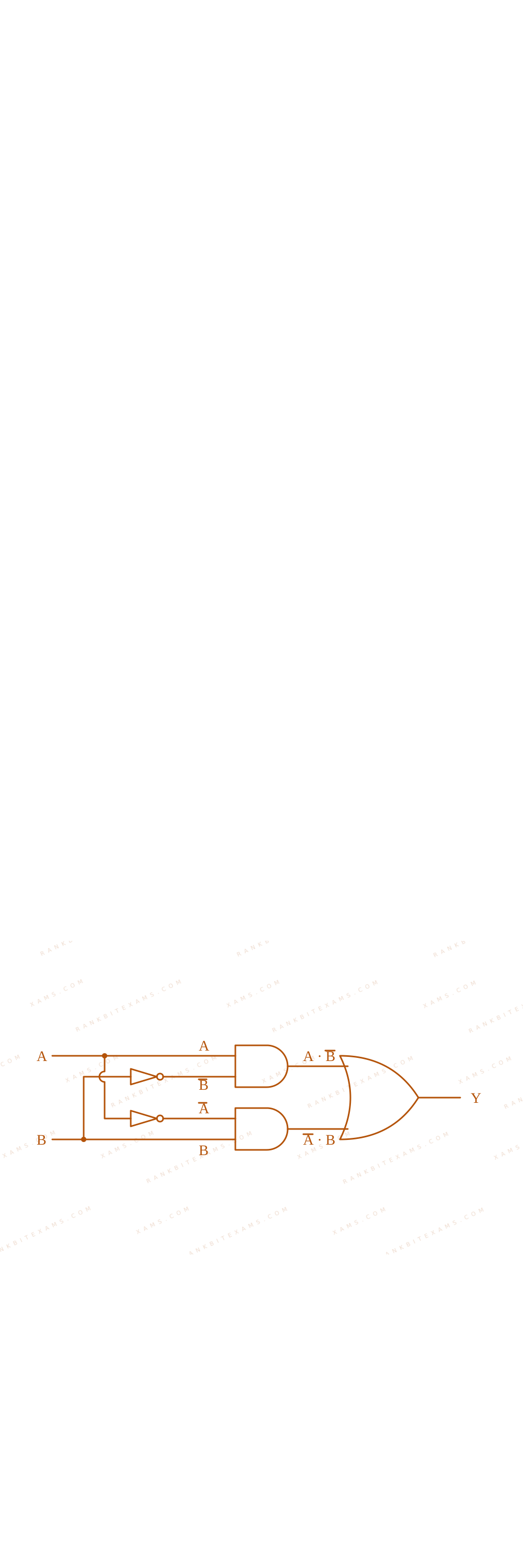
The image shows a digital logic circuit containing multiple interconnected logic gates with input terminals A and B and output terminal Y.
  • A. array|c|c|c| A & B & Y 0 & 0 & 0 0 & 1 & 1 1 & 0 & 1 1 & 1 & 0 array
  • B. array|c|c|c| A & B & Y 0 & 0 & 0 1 & 0 & 0 1 & 1 & 0 0 & 1 & 1 array
  • C. array|c|c|c| A & B & Y 0 & 0 & 0 1 & 0 & 1 0 & 1 & 0 1 & 1 & 0 array
  • D. array|c|c|c| A & B & Y 0 & 0 & 0 1 & 1 & 1 1 & 0 & 1 0 & 1 & 1 array

Solution

Related Formula
Y = A · B + A · B = A B
Core Logic

Analyzing the circuit layout:

  • The top AND gate receives inputs A and B, yielding output term A B.
  • The bottom AND gate receives inputs A and B, yielding output term AB.
  • These terms pass into a terminal OR gate, producing:
Y = A B + AB

Logic Boolean Analysis diagram for Q18 - JEE Main 2025 Evening
The image shows a digital logic circuit containing multiple interconnected logic gates with input terminals A and B and output terminal Y.
Logic Boolean Analysis diagram for Q18 - JEE Main 2025 Evening
The image shows a digital logic circuit containing multiple interconnected logic gates with input terminals A and B and output terminal Y.

This is the precise expression for an XOR (Exclusive OR) gate. The corresponding truth table gives an output of 1 only when inputs are mismatched (0,1 or 1,0), and 0 otherwise. This aligns exactly with Option 1.

Pattern Recognition

Recognize the symmetric cross-inversion network of gates: (A · B) + ( A · B). This combination structurally builds an XOR logic function.

Chapter Mix

Class 12 Physics: Semiconductor Electronics

More Semiconductor Electronics Questions — jee_main_2025_29_jan_morning

Practice all Semiconductor Electronics previous-year questions →

Rankbit System
JEE Physics: Waves (+15.5%) | Electrostatics: Concentric Shells (-29.7%) | Modern Physics: Photoelectric Clones (+34.2%) | Mathematics: Definite Integrals (+18.1%) | Chemistry: Coordination Splitting (-11.4%) | JEE Physics: Waves (+15.5%) | Electrostatics: Concentric Shells (-29.7%) | Modern Physics: Photoelectric Clones (+34.2%) | Mathematics: Definite Integrals (+18.1%) | Chemistry: Coordination Splitting (-11.4%)