
Consider the following statements: A. The junction area of solar cell is made very narrow compared to a photo diode. B. Solar cells are not connected with any external bias. C. LED is made of lightly doped p-n junction. D. Increase of forward current results in continuous increase of LED light intensity. E. LEDs have to be connected in forward bias for emission of light. Choose the correct answer from the options given below :

Solution & Explanation

Core Logic

Let's analyze each statement conceptually: Statement A: Solar cells require a wide surface layer area to intercept maximum sunlight illumination, so junction area is large.

  • Statement B: True. Solar cells operate spontaneously to provide power to loads without requiring external bias voltage.
  • Statement C: False. LEDs are made of heavily doped junctions to maximize recombination probability.
  • Statement D: False. Beyond a critical limit, high currents cause heating that drops efficiency, so emission intensity does not increase infinitely.
  • Statement E: True. Forward biasing allows minority injection leading to radiative recombination.
Step 1: Selecting Option

Since statements B and E are purely accurate, the correct grouping option is B, E Only.

Pattern Recognition

Remember: LEDs = Forward Bias, Photodiodes = Reverse Bias, Solar Cells = Zero External Bias.

Chapter Mix

Class 12 Physics: Semiconductor Electronics: Materials, Devices and Simple Circuits

Reference Study Guides

More Semiconductor Electronics: Materials, Devices and Simple Circuits Previous-Year Questions — Page 7

Q49 jee_main_2024_31_jan_evening Logic Gates
The output of the given circuit diagram is
Logic Gates diagram for Q49 - JEE Main 2024 Evening
The image shows a logic circuit composed of NOT gates, OR gates, and a final NOR gate.
  • A.
    ABY
    000
    100
    010
    111
  • B.
    ABY
    000
    101
    011
    110
  • C.
    ABY
    000
    100
    010
    110
  • D.
    ABY
    000
    100
    011
    110

Solution

Related Formula

Boolean Algebra expressions for logic gates: NOT: A OR: A + B NOR: A + B

Core Logic

Analyze the paths from inputs A and B to the final output Y.
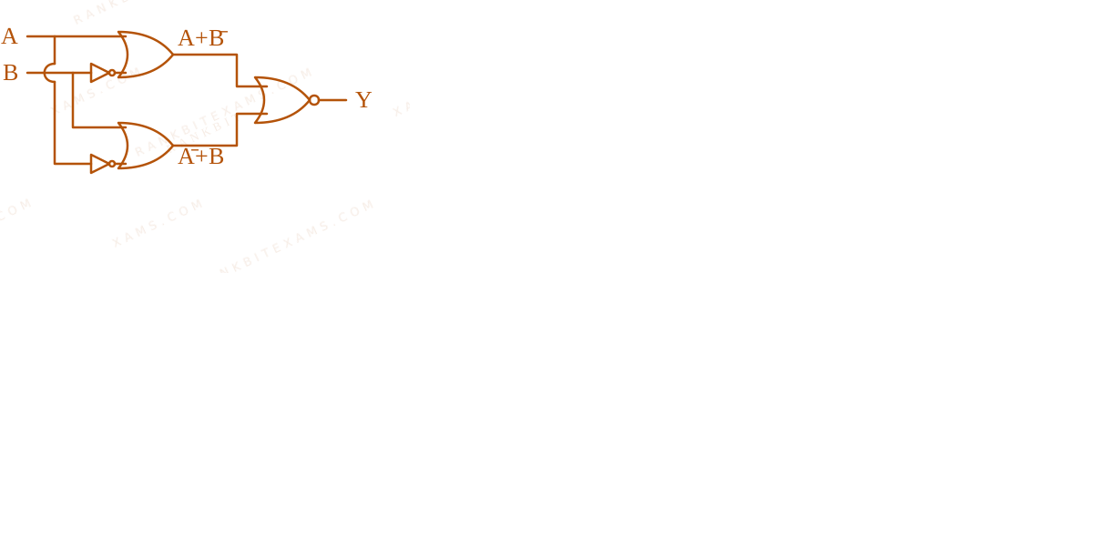
Logic Gates diagram for Q49 - JEE Main 2024 Evening
The image shows a logic circuit composed of NOT gates, OR gates, and a final NOR gate.

Step 1: Intermediate Signals

Top OR gate inputs: A directly, and B inverted (B). Top OR gate output: A + B

Bottom OR gate inputs: A inverted (A), and B directly. Bottom OR gate output: A + B

Step 2: Final Gate Evaluation

The final gate is a NOR gate taking the two intermediate outputs as its inputs.

Y = (A + B) + ( A + B)

Notice that the inner sum simplifies cleanly:

(A + A) + (B + B)

Since A + A = 1 and B + B = 1, the inner term is 1 + 1 = 1.

Y = 1 = 0
Step 3: Conclusion

The output Y is always 0 regardless of the inputs A and B. Checking the truth tables, only option 3 satisfies Y=0 for all conditions.

Pattern Recognition

When a Boolean expression groups a variable and its exact complement together in an OR configuration (A and A), the result instantly hits logic 1. Feeding 1 into any NOR gate guarantees a 0 output universally.

Chapter Mix

Class 12 Physics: Semiconductor Electronics
Q jee_main_2024_31_jan_morning Logic Gates
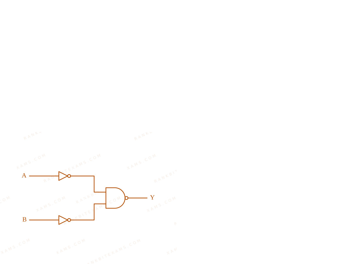
Identify the logic operation performed by the given circuit.
Logic Gates diagram for Q32 - JEE Main 2024 Morning
Two inputs passing through NOT gates before entering a NAND gate.
  • A. NAND
  • B. NOR
  • C. OR
  • D. AND

Solution

Related Formula
Y = A · B (NAND) Y = A + B (De Morgan's)
Core Logic

The inputs A and B are first passed through individual NOT gates (made from tied-input NAND gates or standard NOT gates). The outputs become A and B.

These are then fed into a NAND gate. The final output Y is:

Y = A · B

Applying De-Morgan's Law:

Y = A + B

Y = A + B

This represents an OR operation.

Pattern Recognition

Bubbled inputs on a NAND gate convert it directly into an OR gate via De-Morgan's laws. (Bubbled NAND = OR).

Chapter Mix

Class 12 Physics: Semiconductor Electronics

More Semiconductor Electronics: Materials, Devices and Simple Circuits Questions — jee_main_2025_24_jan_morning

Practice all Semiconductor Electronics: Materials, Devices and Simple Circuits previous-year questions →

Rankbit System
JEE Physics: Waves (+15.5%) | Electrostatics: Concentric Shells (-29.7%) | Modern Physics: Photoelectric Clones (+34.2%) | Mathematics: Definite Integrals (+18.1%) | Chemistry: Coordination Splitting (-11.4%) | JEE Physics: Waves (+15.5%) | Electrostatics: Concentric Shells (-29.7%) | Modern Physics: Photoelectric Clones (+34.2%) | Mathematics: Definite Integrals (+18.1%) | Chemistry: Coordination Splitting (-11.4%)