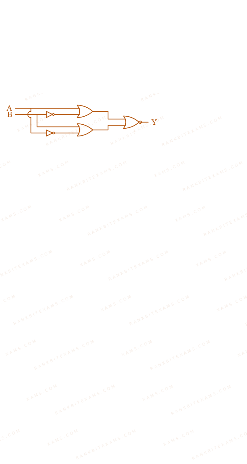
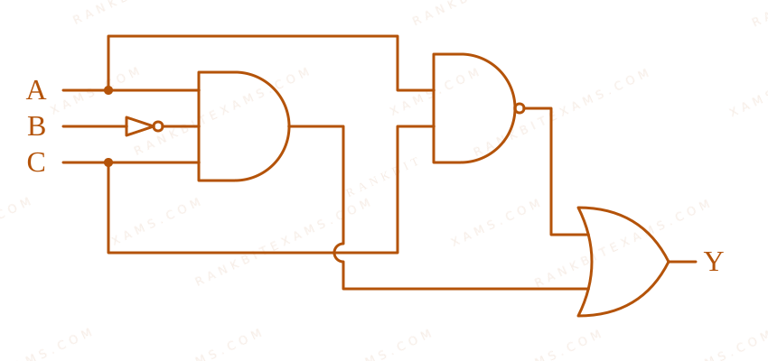
The output of the given circuit diagram is
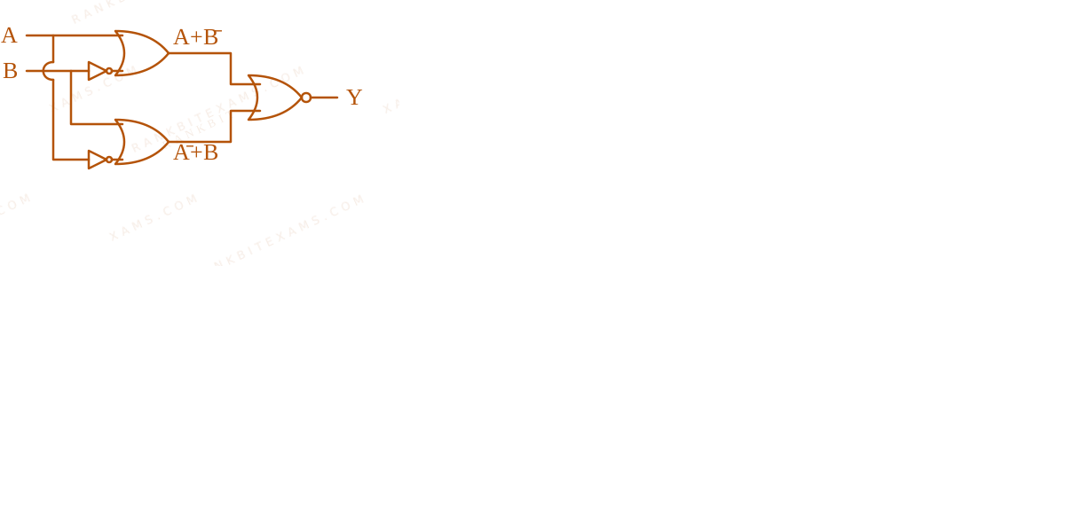
The image shows a logic circuit composed of NOT gates, OR gates, and a final NOR gate.
A.
A
B
Y
0
0
0
1
0
0
0
1
0
1
1
1
B.
A
B
Y
0
0
0
1
0
1
0
1
1
1
1
0
C.
A
B
Y
0
0
0
1
0
0
0
1
0
1
1
0
D.
A
B
Y
0
0
0
1
0
0
0
1
1
1
1
0
Solution & Explanation
Related Formula
Boolean Algebra expressions for logic gates:
NOT: A$\overline{A}$
OR: A + B$A + B$
NOR: A + B$\overline{A + B}$
Core Logic
Analyze the paths from inputs A and B to the final output Y.
The image shows a logic circuit composed of NOT gates, OR gates, and a final NOR gate.
Step 1: Intermediate Signals
Top OR gate inputs: A$A$ directly, and B$B$ inverted (B$\overline{B}$).
Top OR gate output: A + B$A + \overline{B}$
Bottom OR gate inputs: A$A$ inverted (A$\overline{A}$), and B$B$ directly.
Bottom OR gate output: A + B$\overline{A} + B$
Step 2: Final Gate Evaluation
The final gate is a NOR gate taking the two intermediate outputs as its inputs.
Y = (A + B) + ( A + B)$$Y = \overline{(A + \overline{B}) + (\overline{A} + B)}$$
Notice that the inner sum simplifies cleanly:
(A + A) + (B + B)$$(A + \overline{A}) + (B + \overline{B})$$
Since A + A = 1$A + \overline{A} = 1$ and B + B = 1$B + \overline{B} = 1$, the inner term is 1 + 1 = 1$1 + 1 = 1$.
Y = 1 = 0$$Y = \overline{1} = 0$$
Step 3: Conclusion
The output Y is always 0 regardless of the inputs A and B. Checking the truth tables, only option 3 satisfies Y=0$Y=0$ for all conditions.
Pattern Recognition
When a Boolean expression groups a variable and its exact complement together in an OR configuration (A$A$ and A$\overline{A}$), the result instantly hits logic 1. Feeding 1 into any NOR gate guarantees a 0 output universally.
Keywords:#circuit diagram#logic gates#JEE Main 2024 Evening Q49#Semiconductor Electronics JEE Main 2024#Logic Gates JEE Main 2024#OR gate#NOR gate#NOT gate
More Semiconductor Electronics Previous-Year Questions — Page 4
Qjee_main_2025_28_jan_morningLogic Gates
Which of the following circuits has the same output as that of the given circuit?
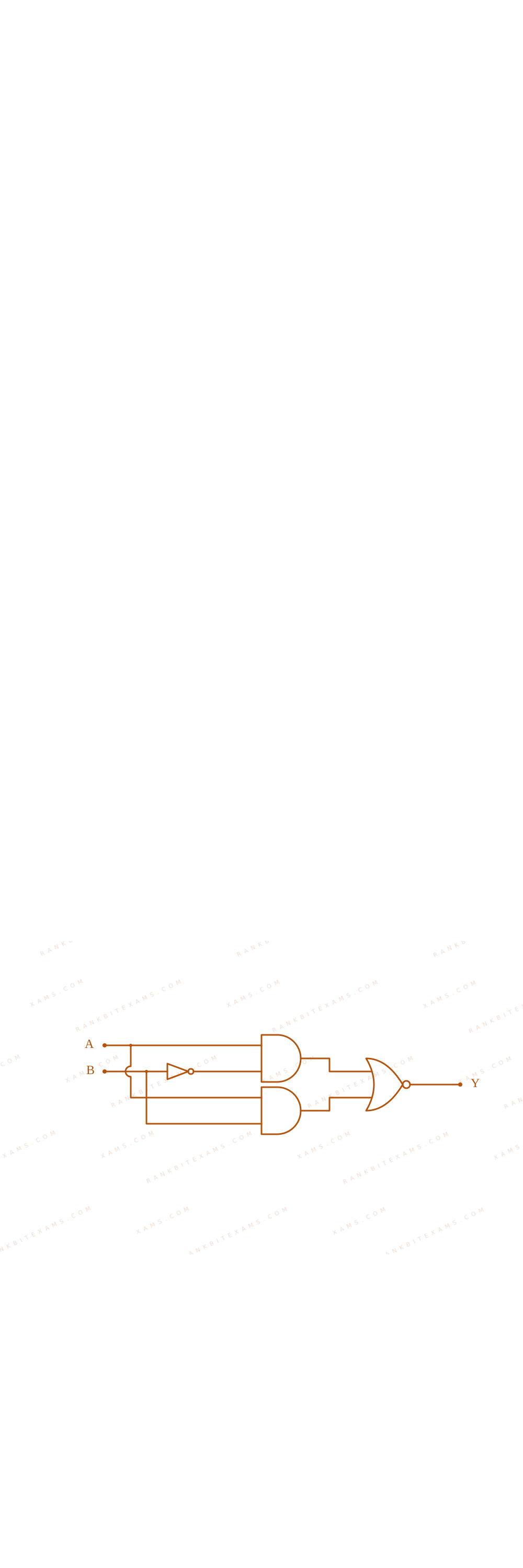
A combination gate circuit configuration evaluated for total Boolean output expressions.
A.
B.
C.
D.
Solution
Core Logic
Let's perform Boolean analysis on the configuration steps mapped below:
P = A · B$$\mathrm{P} = \mathrm{A} \cdot \bar{\mathrm{B}}$$Q = A · B$$\mathrm{Q} = \mathrm{A} \cdot \mathrm{B}$$Y = P + Q = A · B + A · B$$\mathrm{Y} = \overline{\mathrm{P} + \mathrm{Q}} = \overline{\mathrm{A} \cdot \bar{\mathrm{B}} + \mathrm{A} \cdot \mathrm{B}}$$
Factoring using distributive Boolean rules:
Y = A · (B + B) = A · 1$$\mathrm{Y} = \overline{\mathrm{A} \cdot (\mathrm{B} + \bar{\mathrm{B}})} = \overline{\mathrm{A} \cdot 1}$$Y = A$$\mathrm{Y} = \bar{\mathrm{A}}$$
Step 1: Final Reduction
The expression reduces to a simple inverter (NOT gate) processing input A. This aligns with Circuit (1), matching option (1).
Pattern Recognition
Identify standard combinations: (A AND NOT B) OR (A AND B)$(\mathrm{A} \text{ AND NOT } \mathrm{B}) \text{ OR } (\mathrm{A} \text{ AND } \mathrm{B})$ collapses back into simply input A because operand B covers all possible states.
Chapter Mix
Class 12 Physics: Semiconductor Electronics: Materials, Devices and Simple Circuits
Qjee_main_2025_03_april_morningLogic Gates
Choose the correct logic circuit for the given truth table having inputs A and B.
Inputs
Output
A$A$
B$B$
Y$Y$
0
0
0
0
1
0
1
0
1
1
1
1
A.
B.
C.
D.
Solution
Related Formula
Let us inspect the Boolean expression for the output Y$Y$ from the truth table.
From the table:
If A=0$A=0$, Y=0$Y=0$ regardless of B$B$.
If A=1$A=1$, Y=1$Y=1$ regardless of B$B$.
Thus, the truth table is represented by the simple direct logical equation:
Y = A$Y = A$
Core Logic
Let's check the Boolean output of the options shown in the question paper:
Circuit (1): Inputs A$A$ and B$B$ go into an OR gate, outputting (A + B)$(A + B)$. This output and B$B$ then go to an AND gate.
Y = (A + B) · B = A· B + B· B = B(A + 1) = B$$Y = (A + B) \cdot B = A\cdot B + B\cdot B = B(A + 1) = B$$
This gives Y = B$Y = B$ (Not matching table).
Circuit (2): Inputs A$A$ and B$B$ go into an OR gate, outputting (A + B)$(A + B)$. This and A$A$ then go into an AND gate.
Y = (A + B) · A = A· A + A· B = A + A· B = A(1 + B) = A$$Y = (A + B) \cdot A = A\cdot A + A\cdot B = A + A\cdot B = A(1 + B) = A$$
This gives Y = A$Y = A$ (Perfect match to the truth table where Y$Y$ exactly copies A$A$).
Step 1: Verification of Circuit (2)
Let's double-check the truth table values for Circuit (2):
This perfectly matches the given truth table. Therefore, Circuit (2) is correct.
Pattern Recognition
Identify the logic expression directly from the truth table first! Notice that Y$Y$ is completely independent of B$B$ and strictly equals A$A$. This immediately points to any Boolean simplification that collapses to A$A$ (such as absorption law: A(A+B) = A$A(A+B) = A$).
Chapter Mix
Class 12 Physics: Semiconductor Electronics: Materials, Devices and Simple Circuits
Consider a n-type semiconductor in which nₑ$n_{e}$ and nh$n_{h}$ are number of electrons and holes, respectively.
(A) Holes are minority carriers
(B) The dopant is a pentavalent atom
(C) nₑnh≠ nᵢ²$n_{e}n_{h}\ne n_{i}^{2}$ (where nᵢ$n_{i}$ is number of electrons or holes in semiconductor when it is in intrinsic form)
(D) nₑnh≥ nᵢ²$n_{e}n_{h}\ge n_{i}^{2}$
(E) The holes are not generated due to the donors
Choose the correct answer from the options given below:
A. (A), (C), (D) only
B. (A), (C), (E) only
C. (A), (B), (E) only
D. (A), (B), (C) only
Solution
Related Formula
Mass Action Law:
nₑ · nh = nᵢ²$$n_e \cdot n_h = n_i^2$$
Core Logic
Let's analyze each statement for an n-type semiconductor:
(A) Holes are minority carriers: True, electrons are the majority carriers.
(B) The dopant is a pentavalent atom: True (like Phosphorus, Arsenic) which provides extra free electrons.
(C) and (D) contradict the fundamental mass action law nₑ nh = nᵢ²$n_e n_h = n_i^2$, so they are False.
(E) Holes are generated purely due to thermal excitation, not due to donor atoms: True.
Step 1: Assemble Correct Set
Statements (A), (B), and (E) are explicitly correct.
Pattern Recognition
Mass action law (nₑ nh = nᵢ²$n_e n_h = n_i^2$) holds uniformly for both doped types at thermal equilibrium. In n-type systems, donors directly inject electrons only; holes emerge solely from thermal breakages of lattice bonds.
Chapter Mix
Class 12 Physics: Semiconductor Electronics
Qjee_main_2025_04_april_morningLogic Gates
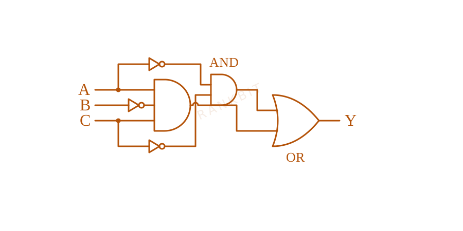
The Boolean expression Y=AoverlineBC+overlineAoverlineC$Y=Aoverline{B}C+overline{A}overline{C}$ can be realised with which of the following gate configurations.
A. One 3-input AND gate, 3 NOT gates and one 2-input OR gate, One 2-input AND gate
B. One 3-input AND gate, 1 NOT gate, One 2-input NOR gate and one 2-input OR gate
C. 3-input OR gate, 3 NOT gates and one 2-input AND gate
Choose the correct answer from the options given below
A. B, C Only
B. A, B Only
C. A, B, C Only
D. A, C Only
Solution
Related Formula
Given logical expression:
Y = A BC + A C$$Y = A\overline{B}C + \overline{A}\overline{C}$$
Configuration A: Generates A BC$A\overline{B}C$ using one 3-input AND gate and one NOT gate for input B$B$. Generates A C$\overline{A}\overline{C}$ using one 2-input AND gate and two separate NOT gates for inputs A$A$ and C$C$. Combines both terms using a 2-input OR gate.
(Total: one 3-input AND, one 2-input AND, three NOT gates, one 2-input OR gate).
Logic circuit layout A for Q15 - JEE Main 2025 Morning
Step 1: Verify Configuration B
Configuration B: Generates A BC$A\overline{B}C$ using one 3-input AND gate and one NOT gate for input B$B$. Simplifies the second term A C$\overline{A}\overline{C}$ into A+C$\overline{A+C}$, realized directly with a single 2-input NOR gate. Combines both sub-circuits using a 2-input OR gate.
(Total: one 3-input AND, one 2-input NOR, one NOT gate, one 2-input OR gate).
Logic circuit layout A for Q15 - JEE Main 2025 Morning
Step 2: Verify Configuration C
Configuration C: Specifies a 3-input OR gate and a 2-input AND gate at the output, which implements a product-of-sums form rather than the required sum-of-products expression. Hence, Configuration C is invalid.
Both configurations A and B correctly realize the logic function.
Pattern Recognition
Apply De Morgan's theorem (A· B = A+B$\overline{A}\cdot\overline{B} = \overline{A+B}$) to convert negated AND products into standard NOR gate structures, reducing the total gate count.
Evaluation Rubric / Model Answer
Option B: A, B Only
Chapter Mix
Class 12 Physics: Semiconductor Electronics
Q11jee_main_2025_07_april_eveningLogic Gates
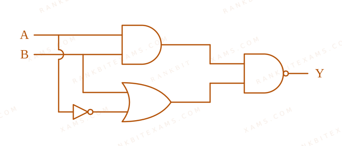
Consider the following logic circuit.
The diagram illustrates a combination of an AND gate, an inverter, an OR gate, and a terminal NAND gate with inputs A and B.
The output is Y=0$Y=0$ when : [cite: 64, 89]
A. A=1 and B=1 [cite: 90]
B. A=0 and B=1 [cite: 99]
C. A=1 and B=0 [cite: 91]
D. A=0 and B=0 [cite: 100]
Solution
Core Logic
Let the intermediate outputs of the first layers be Y₁$Y_1$ and Y₂$Y_2$ [cite: 747]:
Top gate is an AND gate with inputs A$A$ and B$B$, so Y₁ = A · B$Y_1 = A \cdot B$ [cite: 747].
Bottom gate is an OR gate where one input is B$B$ and the other is A$\bar{A}$ via a NOT gate, so Y₂ = A + B$Y_2 = \bar{A} + B$ [cite: 747].
The final layer is a NAND gate with inputs Y₁$Y_1$ and Y₂$Y_2$, so Y = Y₁ · Y₂$Y = \overline{Y_1 \cdot Y_2}$[cite: 748].
Step 1: Constructing the Truth Table
Let's compute the output Y$Y$ for all binary input pairs (A, B)$(A, B)$ [cite: 757]:
Thus, Y=0$Y=0$ uniquely when A=1$A=1$ and B=1$B=1$[cite: 89, 90, 757].
Pattern Recognition
A NAND gate produces an output of 0$0$ if and only if all its inputs are 1$1$. Working backward, this instantly sets Y₁=1$Y_1=1$ and Y₂=1$Y_2=1$. For Y₁ = A · B = 1$Y_1 = A \cdot B = 1$, we must have A=1$A=1$ and B=1$B=1$ simultaneously.
Chapter Mix
Class 12 Physics: Semiconductors
More Semiconductor Electronics Questions — jee_main_2024_31_jan_evening
Practice past-year questions one chapter at a time. Pick an exam → subject → chapter and get every PYQ for that topic — pulled together from all past papers — with the chapter's key formulas alongside.