Rankbit System
JEE Physics: Waves (+15.5%) | Electrostatics: Concentric Shells (-29.7%) | Modern Physics: Photoelectric Clones (+34.2%) | Mathematics: Definite Integrals (+18.1%) | Chemistry: Coordination Splitting (-11.4%) | JEE Physics: Waves (+15.5%) | Electrostatics: Concentric Shells (-29.7%) | Modern Physics: Photoelectric Clones (+34.2%) | Mathematics: Definite Integrals (+18.1%) | Chemistry: Coordination Splitting (-11.4%)

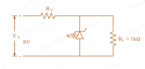
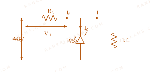
In the given circuit if the power rating of Zener diode is 10mathrm~mW, the value of series resistance R_s to regulate the input unregulated supply is:
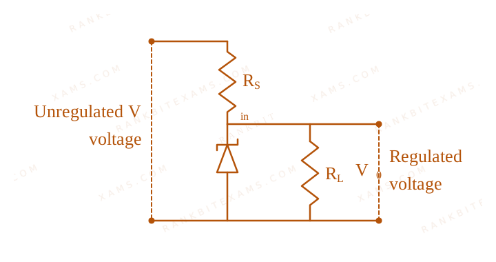
Zener Diode voltage regulation circuit for Q33 - JEE Main 2024 Morning
The diagram illustrates a Zener diode stabilizer network with an unregulated input supply of 8V, a Zener voltage of 5V, a series resistor Rs, and a load resistor RL of 1 kOhm.

Solution & Explanation

### Related Formula Voltage drop across series resistor: V_s = V_textin - V_Z Load current: I_L = fracV_ZR_L Maximum Zener current: I_Ztextmax = fracP_ZV_Z ### Core Logic Given values: V_textin = 8mathrm~V, V_Z = 5mathrm~V, R_L = 1mathrm~kOmega, P_Z = 10mathrm~mW. Voltage across R_s: V_R_s = 8 - 5 = 3mathrm~V Current through the load resistor: I_L = frac51 times 10^3 = 5mathrm~mA Maximum current allowed through the Zener diode: I_Ztextmax = frac10 times 10^-35 = 2mathrm~mA ### Step 1: Determine the Range of Resistance Total current through the series loop: I_s = I_Z + I_L For maximum safety configuration (Zener operating at peak current): I_stextmax = I_Ztextmax + I_L = 2mathrm~mA + 5mathrm~mA = 7mathrm~mA R_stextmin = fracV_R_sI_stextmax = frac3mathrm~V7mathrm~mA = frac37mathrm~kOmega approx 428.6mathrm~Omega For minimum Zener current requirement (I_Z to 0): I_stextmin = 0 + 5mathrm~mA = 5mathrm~mA R_stextmax = fracV_R_sI_stextmin = frac3mathrm~V5mathrm~mA = frac35mathrm~kOmega = 600mathrm~Omega Therefore, the required window for regulation is: frac37mathrm~kOmega < R_s < frac35mathrm~kOmega ### Step 2: Note on Official Key None of the given multiple-choice options fall strictly within the stable bounds [428.6mathrm~Omega, 600mathrm~Omega]. Officially, the answer key evaluates option (3) as correct, though the problem functions fundamentally as a bonus candidate under rigorous design tolerances. ### Pattern Recognition Always solve the current constraints at both boundaries (I_Z = 0 and I_Z = I_textmax) to bracket the allowable series resistor zone. ### Evaluation Rubric / Model Answer null ### Chapter Mix Class 12 Physics: Semiconductor Electronics
Detailed currents in Zener stabilizer solution path for Q33
The diagram illustrates a Zener diode stabilizer network with an unregulated input supply of 8V, a Zener voltage of 5V, a series resistor Rs, and a load resistor RL of 1 kOhm.

Reference Study Guides

More Semiconductor Electronics Previous-Year Questions

Q13 jee_main_2025_02_april_evening Logic Gates
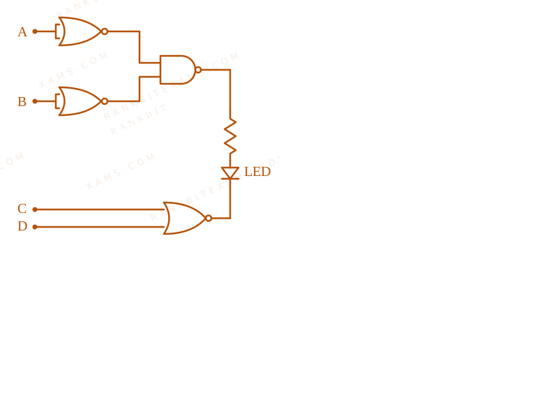
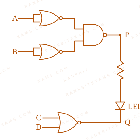
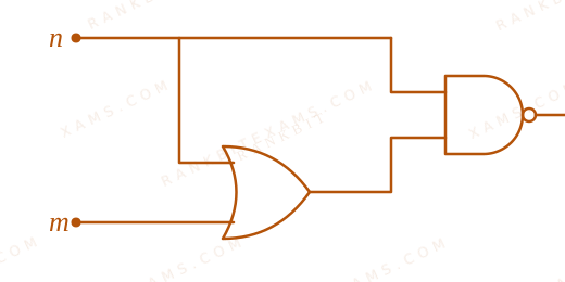
In the digital circuit shown in the figure, for the given inputs the P and Q values are :
Digital logic gate circuit diagram with inputs 1 and 1
The circuit has two inputs equal to 1, passing through multiple gates to produce outputs P and Q.
  • A. mathrmP = 1, mathrmQ = 1
  • B. mathrmP = 0, mathrmQ = 0
  • C. mathrmP = 0, mathrmQ = 1
  • D. mathrmP = 1, mathrmQ = 0

Solution

### Related Formula Truth relations of basic logic operations: - NAND operation: Y = overlineA cdot B - NOR operation: Y = overlineA + B - NOT operation: Y = overlineA - OR operation: Y = A + B ### Core Logic The inputs are: - Top input = 1 - Bottom input = 1 Let's analyze step-by-step from left to right: 1. **First Gate (NAND gate at the top-left):** - Inputs are 1 and 1. - Output = overline1 cdot 1 = 0. 2. **Bottom-left path with NOT gates:** - Top input (1) goes to a NOT gate, producing 0. - Bottom input (1) goes to a NOT gate, producing 0. - These two 0 values feed into the OR gate: - Output = 0 + 0 = 0. ### Step 1: Calculate output P Now trace the path to P: - The inputs to the top-right AND gate are: - Output of the top-left NAND gate = 0 - Output of the bottom-left OR gate = 0 - Therefore, output P is: P = 0 cdot 0 = 0 ### Step 2: Calculate output Q Now trace the path to Q: - The gate at the bottom-right is a NOR gate with two inputs: - Input 1: Output of the top-left NAND gate (0) inverted by a NOT gate = overline0 = 1. - Input 2: Output of the bottom-left OR gate (0). - Passing these inputs (1 and 0) through the final NOR gate: Q = overline1 + 0 = overline1 = 0 Thus, both P = 0 and Q = 0. ### Pattern Recognition Sees: Combinational trace with inverted nodes. Trap: Missing bubbles (NOT gates) representing inversion on internal circuit paths. Shortcut: The first NAND gate output is 0 (since both inputs are 1). This 0 directly goes to the upper AND gate, immediately guaranteeing output P = 0 (eliminates options 1 and 4). Now, you only need to evaluate Q to choose between options 2 and 3. ### Evaluation Rubric / Model Answer null ### Chapter Mix Class 12 Physics: Semiconductor Electronics: Materials, Devices and Simple Circuits
Q11 jee_main_2025_07_april_morning Zener Diode
In the following circuit, the reading of the ammeter will be (Take Zener breakdown voltage = 4 V)
Zener regulator circuit for Q11 - JEE Main 2025 Morning
A schematic showing a 12V supply connected to a series 100 ohm resistor, which then branches into a parallel Zener diode and a 400 ohm resistor in series with an ammeter.
  • A. 24mathrmmA
  • B. 80mathrmmA
  • C. 10mathrmmA
  • D. 60mathrmmA

Solution

### Related Formula Voltage division across load R_L with series resistance R_s without Zener regulation: V_L = V_textin left( fracR_LR_s + R_L right) If V_L > V_z, the Zener diode enters breakdown, and potential across the parallel load is clamped at V_L = V_z. ### Core Logic Verify if Zener diode operates in the breakdown region: - V_textin = 12 mathrm~V - R_s = 100 Omega - R_L = 400 Omega Calculate the unregulated voltage: V_1 = 12 times left( frac400100 + 400 right) = 12 times frac45 = 9.6 mathrm~V Since V_1 > V_z (9.6 mathrm~V > 4 mathrm~V), breakdown occurs, and the parallel branch voltage is fixed at V_z = 4 mathrm~V. ### Step 1: Calculate Branch Current The voltage across the 400 Omega load resistor (which is in series with the ammeter) is locked at 4 mathrm~V. The current I through the ammeter is: I = fracV_zR_L = frac4 mathrm~V400 Omega = 10^-2 mathrm~A = 10 mathrm~mA ### Pattern Recognition Sees: Parallel Zener diode configuration. Shortcut: Always calculate the open-circuit load voltage first. If it exceeds V_z, use V_z as the branch potential. The branch current is simply V_z / R_L. Here, 4 / 400 = 10 mathrm~mA. ### Evaluation Rubric / Model Answer null ### Chapter Mix Class 12 Physics: Semiconductor Electronics: Materials, Devices and Simple Circuits
Q8 jee_main_2025_08_april_evening Diodes
The output voltage in the following circuit is (Consider ideal diode case)
Diodes circuit diagram for Q8 - JEE Main 2025 Evening
A schematic of a circuit showing an input voltage, two diodes D1 and D2 connected in parallel paths, a resistor, and the output node V_out.
  • A. 10mathrm~V
  • B. 0mathrm~V
  • C. +5mathrm~V
  • D. -5mathrm~V

Solution

### Related Formula For ideal diodes: - **Forward Bias**: Acts as a closed switch (zero resistance, short circuit). - **Reverse Bias**: Acts as an open switch (infinite resistance, open circuit). ### Core Logic Analyzing the bias condition of the diodes based on the applied potential in the schematic: - Diode D_1 is oriented such that its cathode faces the positive terminal (+5mathrm~V), making it **Reverse Biased** (no current flows through this branch). - Diode D_2 is oriented such that its anode connects to the +5mathrm~V path, making it **Forward Biased**. Since D_2 is forward-biased and ideal, it acts as a short circuit (resistance R_D = 0). Current flows through D_2 and through the series resistor. ### Step 1: Calculating output node potential Because the forward-biased ideal diode D_2 connects the node directly to the low-resistance ground loop or the reference resistor drop, the entire 5mathrm~V potential drops across the resistor: V_textout = 0mathrm~V ### Pattern Recognition Sees: Parallel diode configuration with opposite polarities. Shortcut: Check polarity. D_1 is reverse-biased (open), D_2 is forward-biased (short). The output terminal is pulled down to the reference ground, leading directly to 0mathrm~V. ✓ ### Evaluation Rubric / Model Answer null ### Chapter Mix Class 12 Physics: Semiconductor Electronics
Q18 jee_main_2025_29_jan_evening Logic Gates
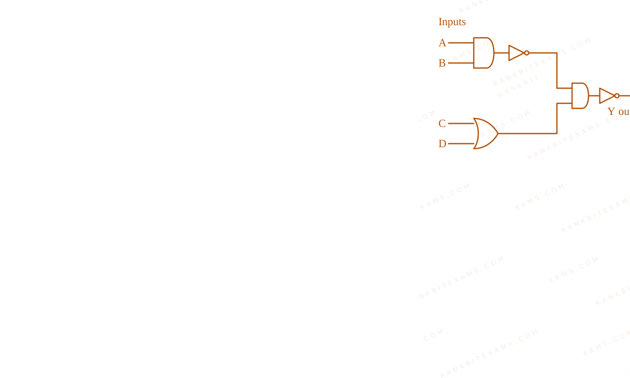
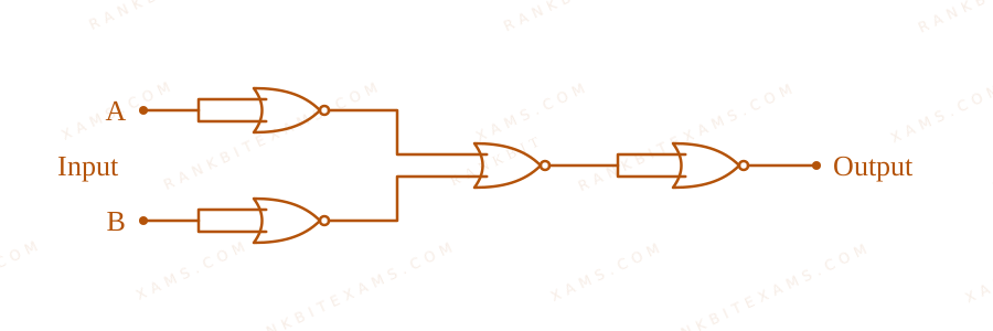
The truth table for the circuit given below is :
Logic Gates circuit diagram for Q18 - JEE Main 2025 Evening
The image shows a digital logic circuit containing multiple interconnected logic gates with input terminals A and B and output terminal Y.
  • A. beginarray|c|c|c| hline A & B & Y \\ hline 0 & 0 & 0 \\ 0 & 1 & 1 \\ 1 & 0 & 1 \\ 1 & 1 & 0 \\ hline endarray
  • B. beginarray|c|c|c| hline A & B & Y \\ hline 0 & 0 & 0 \\ 1 & 0 & 0 \\ 1 & 1 & 0 \\ 0 & 1 & 1 \\ hline endarray
  • C. beginarray|c|c|c| hline A & B & Y \\ hline 0 & 0 & 0 \\ 1 & 0 & 1 \\ 0 & 1 & 0 \\ 1 & 1 & 0 \\ hline endarray
  • D. beginarray|c|c|c| hline A & B & Y \\ hline 0 & 0 & 0 \\ 1 & 1 & 1 \\ 1 & 0 & 1 \\ 0 & 1 & 1 \\ hline endarray

Solution

### Related Formula Y = A cdot barB + barA cdot B = A oplus B ### Core Logic Analyzing the circuit layout: 1. The top AND gate receives inputs A and barB, yielding output term AbarB. 2. The bottom AND gate receives inputs barA and B, yielding output term barAB. 3. These terms pass into a terminal OR gate, producing: Y = AbarB + barAB
Logic Boolean Analysis diagram for Q18 - JEE Main 2025 Evening
The image shows a digital logic circuit containing multiple interconnected logic gates with input terminals A and B and output terminal Y.
Logic Boolean Analysis diagram for Q18 - JEE Main 2025 Evening
The image shows a digital logic circuit containing multiple interconnected logic gates with input terminals A and B and output terminal Y.
This is the precise expression for an **XOR (Exclusive OR) gate**. The corresponding truth table gives an output of 1 only when inputs are mismatched (0,1 or 1,0), and 0 otherwise. This aligns exactly with Option 1. ### Pattern Recognition Recognize the symmetric cross-inversion network of gates: (A cdot barB) + (barA cdot B). This combination structurally builds an XOR logic function. ### Evaluation Rubric / Model Answer null ### Chapter Mix Class 12 Physics: Semiconductor Electronics
Q13 jee_main_2025_28_jan_morning Logic Gates
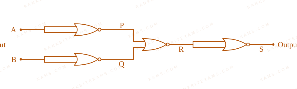
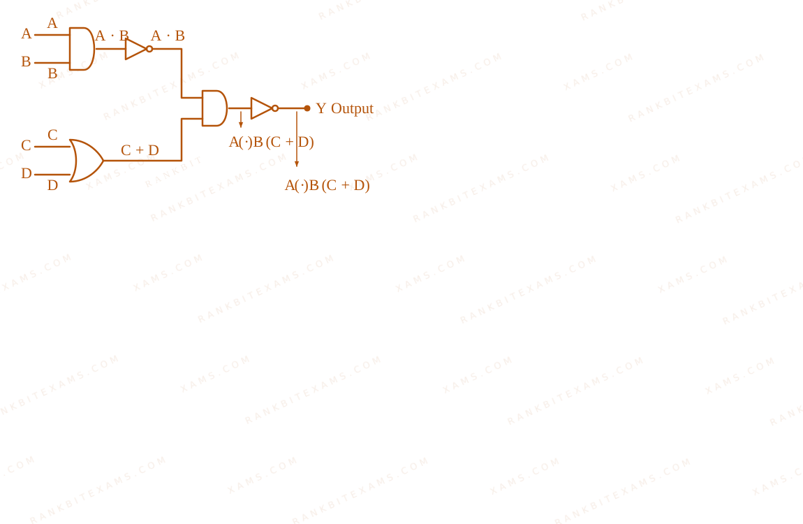
Which of the following circuits has the same output as that of the given circuit?
Logic Gates diagram for Q13 - JEE Main 2025 Morning
A combination gate circuit configuration evaluated for total Boolean output expressions.
  • A. textCircuit (1)
  • B. textCircuit (2)
  • C. textCircuit (3)
  • D. textCircuit (4)

Solution

### Core Logic Let's perform Boolean analysis on the configuration steps mapped below: mathrmP = mathrmA cdot barmathrmB mathrmQ = mathrmA cdot mathrmB mathrmY = overlinemathrmP + mathrmQ = overlinemathrmA cdot barmathrmB + mathrmA cdot mathrmB Factoring using distributive Boolean rules: mathrmY = overlinemathrmA cdot (mathrmB + barmathrmB) = overlinemathrmA cdot 1 mathrmY = barmathrmA ### Step 1: Final Reduction The expression reduces to a simple inverter (NOT gate) processing input A. This aligns with Circuit (1), matching option (1). ### Pattern Recognition Identify standard combinations: (mathrmA text AND NOT mathrmB) text OR (mathrmA text AND mathrmB) collapses back into simply input A because operand B covers all possible states. ### Evaluation Rubric / Model Answer null ### Chapter Mix Class 12 Physics: Semiconductor Electronics: Materials, Devices and Simple Circuits

More Semiconductor Electronics Questions — jee_main_2024_01_february_morning

Practice all Semiconductor Electronics previous-year questions →

YOUR FIRST PREP STEP STARTS HERE

We Map Every Repeating Question in Competitive Exams.

Say goodbye to generic mock test fatigue. RankBit uses smart analysis to group past exam questions into their foundational Repeating Question Types. Find chapter weightage, track repeating questions, and score higher with targeted practice.

Select Your Target Exam

Choose an exam track below to find formulas per chapter and patterns.

Syncing Exam Intelligence

Mapping formulas and patterns across all tracks…

PATH A — FULL LENGTH PRACTICE

Full Mock Test Hub

Simulate real NTA exam conditions with fully tracked mocks. Time yourself against past papers.

Under Development
PATH B — TARGETED PRACTICE

Topic-wise Practice Hub

Practice past-year questions one chapter at a time. Pick an exam → subject → chapter and get every PYQ for that topic — pulled together from all past papers — with the chapter's key formulas alongside.

Loading Questions... Browse Topics
Latest from the Blog
View all →

Loading articles...