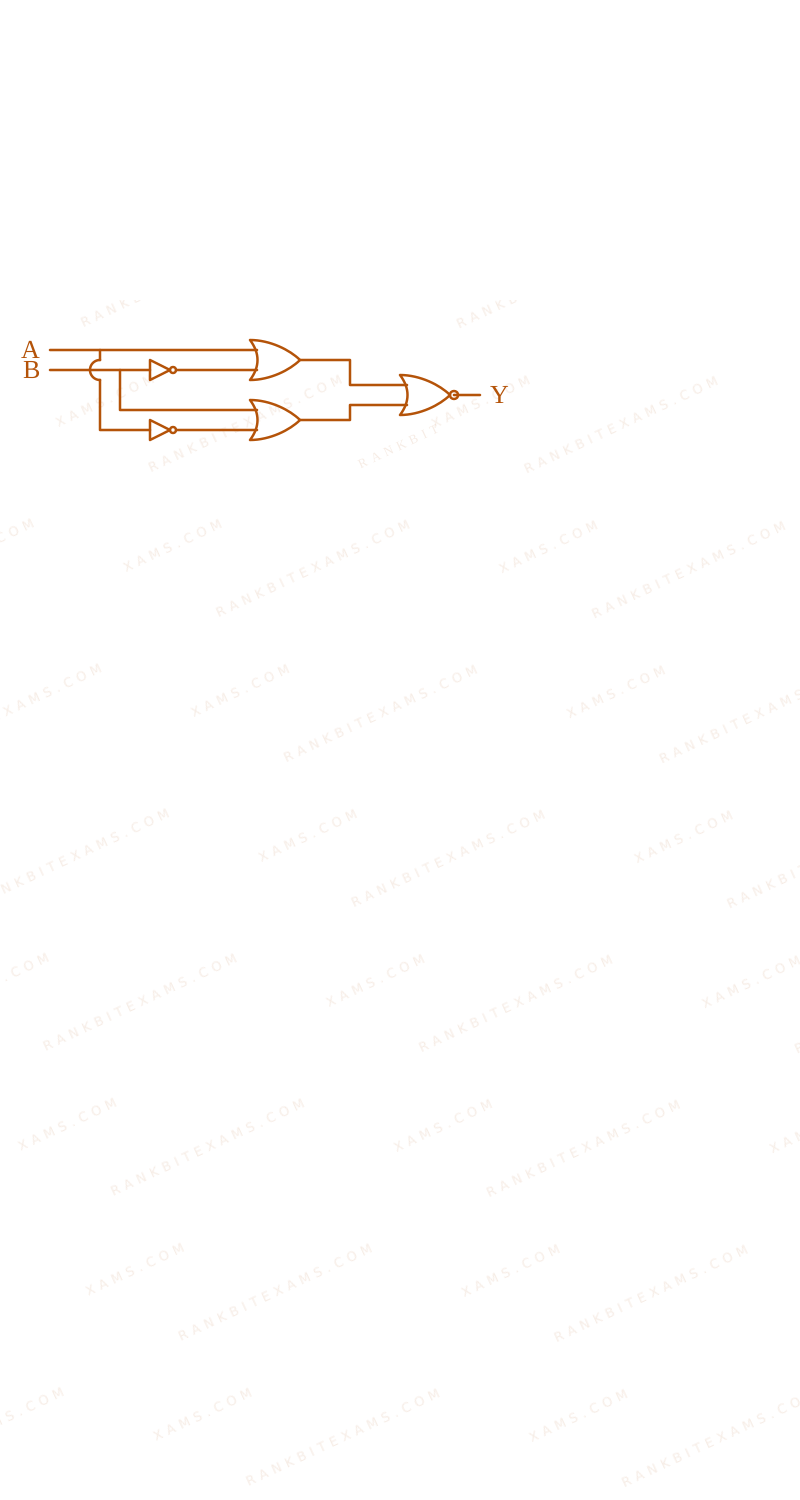
The output of the given circuit diagram is
The image shows a logic circuit composed of NOT gates, OR gates, and a final NOR gate.
A.
A
B
Y
0
0
0
1
0
0
0
1
0
1
1
1
B.
A
B
Y
0
0
0
1
0
1
0
1
1
1
1
0
C.
A
B
Y
0
0
0
1
0
0
0
1
0
1
1
0
D.
A
B
Y
0
0
0
1
0
0
0
1
1
1
1
0
Solution & Explanation
Related Formula
Boolean Algebra expressions for logic gates:
NOT: A$\overline{A}$
OR: A + B$A + B$
NOR: A + B$\overline{A + B}$
Core Logic
Analyze the paths from inputs A and B to the final output Y.
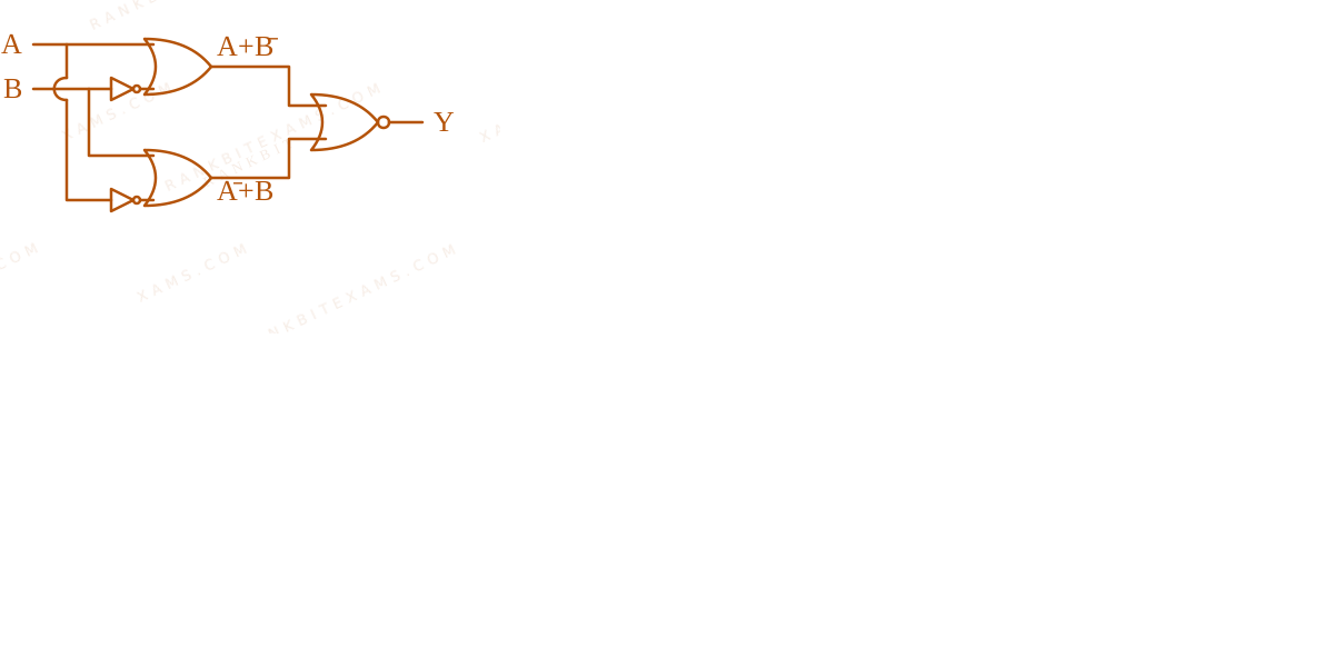
The image shows a logic circuit composed of NOT gates, OR gates, and a final NOR gate.
Step 1: Intermediate Signals
Top OR gate inputs: A$A$ directly, and B$B$ inverted (B$\overline{B}$).
Top OR gate output: A + B$A + \overline{B}$
Bottom OR gate inputs: A$A$ inverted (A$\overline{A}$), and B$B$ directly.
Bottom OR gate output: A + B$\overline{A} + B$
Step 2: Final Gate Evaluation
The final gate is a NOR gate taking the two intermediate outputs as its inputs.
Y = (A + B) + ( A + B)$$Y = \overline{(A + \overline{B}) + (\overline{A} + B)}$$
Notice that the inner sum simplifies cleanly:
(A + A) + (B + B)$$(A + \overline{A}) + (B + \overline{B})$$
Since A + A = 1$A + \overline{A} = 1$ and B + B = 1$B + \overline{B} = 1$, the inner term is 1 + 1 = 1$1 + 1 = 1$.
Y = 1 = 0$$Y = \overline{1} = 0$$
Step 3: Conclusion
The output Y is always 0 regardless of the inputs A and B. Checking the truth tables, only option 3 satisfies Y=0$Y=0$ for all conditions.
Pattern Recognition
When a Boolean expression groups a variable and its exact complement together in an OR configuration (A$A$ and A$\overline{A}$), the result instantly hits logic 1. Feeding 1 into any NOR gate guarantees a 0 output universally.
Keywords:#circuit diagram#logic gates#JEE Main 2024 Evening Q49#Semiconductor Electronics JEE Main 2024#Logic Gates JEE Main 2024#OR gate#NOR gate#NOT gate
More Semiconductor Electronics Previous-Year Questions — Page 7
Qjee_main_2024_31_jan_morningLogic Gates
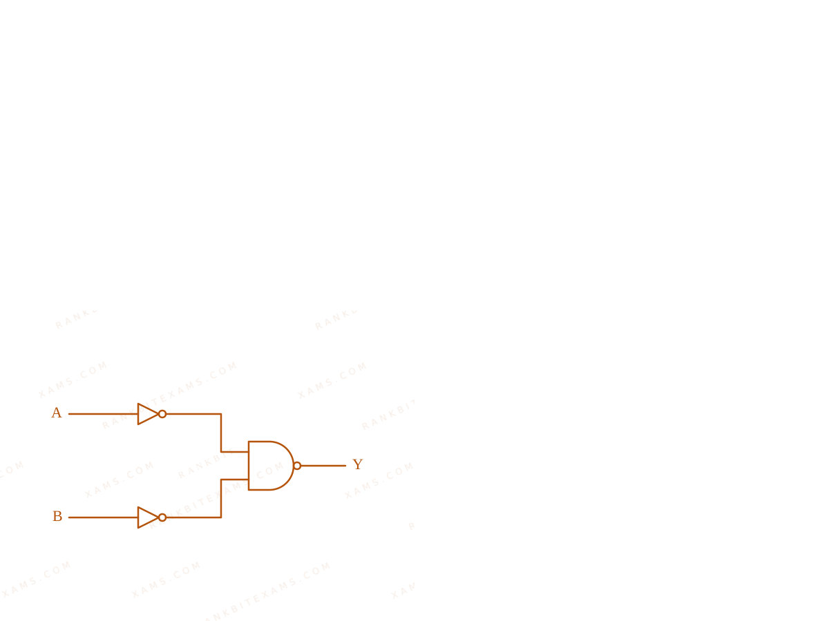
Identify the logic operation performed by the given circuit.
Two inputs passing through NOT gates before entering a NAND gate.
A.NAND$\text{NAND}$
B.NOR$\text{NOR}$
C.OR$\text{OR}$
D.AND$\text{AND}$
Solution
Related Formula
Y = A · B (NAND)$$Y = \overline{A \cdot B} \quad \text{(NAND)}$$Y = A + B (De Morgan's)$$Y = \overline{A} + \overline{B} \quad \text{(De Morgan's)}$$
Core Logic
The inputs A$A$ and B$B$ are first passed through individual NOT gates (made from tied-input NAND gates or standard NOT gates). The outputs become A$\overline{A}$ and B$\overline{B}$.
These are then fed into a NAND gate.
The final output Y$Y$ is:
Y = A · B$$Y = \overline{\overline{A} \cdot \overline{B}}$$
Applying De-Morgan's Law:
Y = A + B$$Y = \overline{\overline{A}} + \overline{\overline{B}}$$
Y = A + B$Y = A + B$
This represents an OR operation.
Pattern Recognition
Bubbled inputs on a NAND gate convert it directly into an OR gate via De-Morgan's laws. (Bubbled NAND = OR).
Chapter Mix
Class 12 Physics: Semiconductor Electronics
More Semiconductor Electronics Questions — jee_main_2024_31_jan_evening
Practice past-year questions one chapter at a time. Pick an exam → subject → chapter and get every PYQ for that topic — pulled together from all past papers — with the chapter's key formulas alongside.