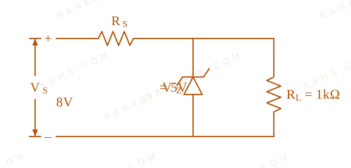
In the given circuit if the power rating of Zener diode is 10~mW, the value of series resistance Rₛ to regulate the input unregulated supply is:
Zener Diode voltage regulation circuit for Q33 - JEE Main 2024 Morning
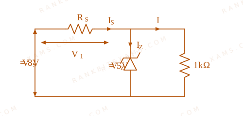
The diagram illustrates a Zener diode stabilizer network with an unregulated input supply of 8V, a Zener voltage of 5V, a series resistor Rs, and a load resistor RL of 1 kOhm.

Solution & Explanation

Related Formula

Voltage drop across series resistor:

Vₛ = Vᵢₙ - VZ

Load current:

IL = (VZ)/(RL)

Maximum Zener current:

IZmax = (PZ)/(VZ)
Core Logic

Given values: Vᵢₙ = 8~V, VZ = 5~V, RL = 1~kΩ, PZ = 10~mW.

Voltage across Rₛ:

VRₛ = 8 - 5 = 3~V

Current through the load resistor:

IL = (5)/(1 × 10³) = 5~mA

Maximum current allowed through the Zener diode:

IZmax = 10 × 10⁻³5 = 2~mA
Step 1: Determine the Range of Resistance

Total current through the series loop: Iₛ = IZ + IL

For maximum safety configuration (Zener operating at peak current):

Ismax = IZmax + IL = 2~mA + 5~mA = 7~mA Rsmin = VRₛIsmax = 3~V7~mA = (3)/(7)~kΩ ≈ 428.6~Ω

For minimum Zener current requirement (IZ → 0):

Ismin = 0 + 5~mA = 5~mA Rsmax = VRₛIsmin = 3~V5~mA = (3)/(5)~kΩ = 600~Ω

Therefore, the required window for regulation is:

(3)/(7)~kΩ < Rₛ < (3)/(5)~kΩ
Step 2: Note on Official Key

None of the given multiple-choice options fall strictly within the stable bounds [428.6~Ω, 600~Ω]. Officially, the answer key evaluates option (3) as correct, though the problem functions fundamentally as a bonus candidate under rigorous design tolerances.

Pattern Recognition

Always solve the current constraints at both boundaries (IZ = 0 and IZ = Imax) to bracket the allowable series resistor zone.

Chapter Mix

Class 12 Physics: Semiconductor Electronics

Detailed currents in Zener stabilizer solution path for Q33
The diagram illustrates a Zener diode stabilizer network with an unregulated input supply of 8V, a Zener voltage of 5V, a series resistor Rs, and a load resistor RL of 1 kOhm.

More Semiconductor Electronics Previous-Year Questions — Page 7

Q49 jee_main_2024_31_jan_evening Logic Gates
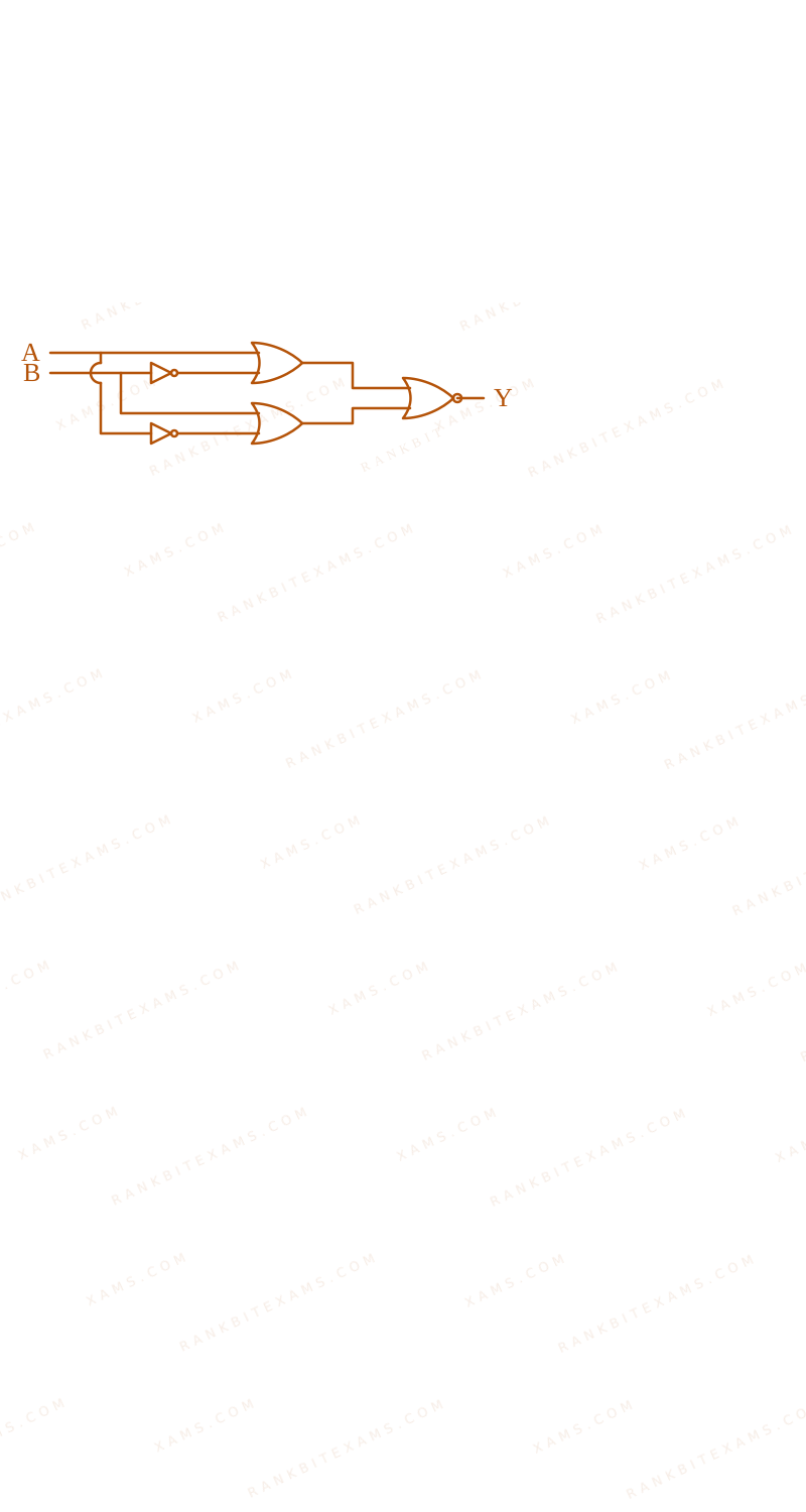
The output of the given circuit diagram is
Logic Gates diagram for Q49 - JEE Main 2024 Evening
The image shows a logic circuit composed of NOT gates, OR gates, and a final NOR gate.
  • A.
    ABY
    000
    100
    010
    111
  • B.
    ABY
    000
    101
    011
    110
  • C.
    ABY
    000
    100
    010
    110
  • D.
    ABY
    000
    100
    011
    110

Solution

Related Formula

Boolean Algebra expressions for logic gates: NOT: A OR: A + B NOR: A + B

Core Logic

Analyze the paths from inputs A and B to the final output Y.
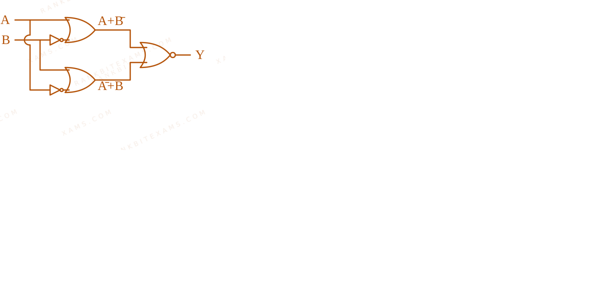
Logic Gates diagram for Q49 - JEE Main 2024 Evening
The image shows a logic circuit composed of NOT gates, OR gates, and a final NOR gate.

Step 1: Intermediate Signals

Top OR gate inputs: A directly, and B inverted (B). Top OR gate output: A + B

Bottom OR gate inputs: A inverted (A), and B directly. Bottom OR gate output: A + B

Step 2: Final Gate Evaluation

The final gate is a NOR gate taking the two intermediate outputs as its inputs.

Y = (A + B) + ( A + B)

Notice that the inner sum simplifies cleanly:

(A + A) + (B + B)

Since A + A = 1 and B + B = 1, the inner term is 1 + 1 = 1.

Y = 1 = 0
Step 3: Conclusion

The output Y is always 0 regardless of the inputs A and B. Checking the truth tables, only option 3 satisfies Y=0 for all conditions.

Pattern Recognition

When a Boolean expression groups a variable and its exact complement together in an OR configuration (A and A), the result instantly hits logic 1. Feeding 1 into any NOR gate guarantees a 0 output universally.

Chapter Mix

Class 12 Physics: Semiconductor Electronics
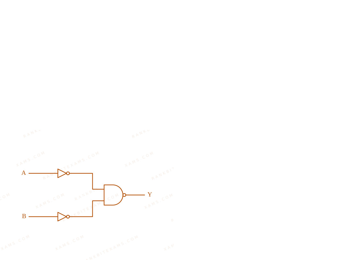
Q jee_main_2024_31_jan_morning Logic Gates
Identify the logic operation performed by the given circuit.
Logic Gates diagram for Q32 - JEE Main 2024 Morning
Two inputs passing through NOT gates before entering a NAND gate.
  • A. NAND
  • B. NOR
  • C. OR
  • D. AND

Solution

Related Formula
Y = A · B (NAND) Y = A + B (De Morgan's)
Core Logic

The inputs A and B are first passed through individual NOT gates (made from tied-input NAND gates or standard NOT gates). The outputs become A and B.

These are then fed into a NAND gate. The final output Y is:

Y = A · B

Applying De-Morgan's Law:

Y = A + B

Y = A + B

This represents an OR operation.

Pattern Recognition

Bubbled inputs on a NAND gate convert it directly into an OR gate via De-Morgan's laws. (Bubbled NAND = OR).

Chapter Mix

Class 12 Physics: Semiconductor Electronics

More Semiconductor Electronics Questions — jee_main_2024_01_february_morning

Practice all Semiconductor Electronics previous-year questions →

Rankbit System
JEE Physics: Waves (+15.5%) | Electrostatics: Concentric Shells (-29.7%) | Modern Physics: Photoelectric Clones (+34.2%) | Mathematics: Definite Integrals (+18.1%) | Chemistry: Coordination Splitting (-11.4%) | JEE Physics: Waves (+15.5%) | Electrostatics: Concentric Shells (-29.7%) | Modern Physics: Photoelectric Clones (+34.2%) | Mathematics: Definite Integrals (+18.1%) | Chemistry: Coordination Splitting (-11.4%)