Rankbit System
JEE Physics: Waves (+15.5%) | Electrostatics: Concentric Shells (-29.7%) | Modern Physics: Photoelectric Clones (+34.2%) | Mathematics: Definite Integrals (+18.1%) | Chemistry: Coordination Splitting (-11.4%) | JEE Physics: Waves (+15.5%) | Electrostatics: Concentric Shells (-29.7%) | Modern Physics: Photoelectric Clones (+34.2%) | Mathematics: Definite Integrals (+18.1%) | Chemistry: Coordination Splitting (-11.4%)

Consider a n-type semiconductor in which n_e and n_h are number of electrons and holes, respectively. (A) Holes are minority carriers (B) The dopant is a pentavalent atom (C) n_en_hne n_i^2 (where n_i is number of electrons or holes in semiconductor when it is in intrinsic form) (D) n_en_hge n_i^2 (E) The holes are not generated due to the donors Choose the correct answer from the options given below:

Solution & Explanation

### Related Formula Mass Action Law: n_e cdot n_h = n_i^2 ### Core Logic Let's analyze each statement for an n-type semiconductor: - (A) Holes are minority carriers: True, electrons are the majority carriers. - (B) The dopant is a pentavalent atom: True (like Phosphorus, Arsenic) which provides extra free electrons. - (C) and (D) contradict the fundamental mass action law n_e n_h = n_i^2, so they are False. - (E) Holes are generated purely due to thermal excitation, not due to donor atoms: True. ### Step 1: Assemble Correct Set Statements (A), (B), and (E) are explicitly correct. ### Pattern Recognition Mass action law (n_e n_h = n_i^2) holds uniformly for both doped types at thermal equilibrium. In n-type systems, donors directly inject electrons only; holes emerge solely from thermal breakages of lattice bonds. ### Evaluation Rubric / Model Answer null ### Chapter Mix Class 12 Physics: Semiconductor Electronics
Reference Study Guides

More Semiconductor Electronics Previous-Year Questions — Page 2

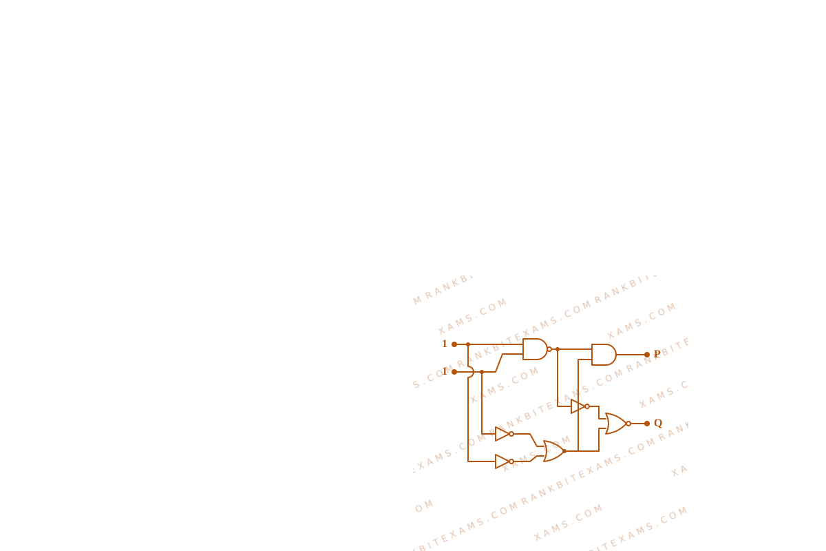
Q15 2025 Logic Gates
The output of the circuit is low (zero) for :
Digital logic gate circuit diagram with inputs X and Y Q15
The figure contains a digital combination logic gate configuration with input variables X and Y.
(A) X = 0, Y = 0 (B) X = 0, Y = 1 (C) X = 1, Y = 0 (D) X = 1, Y = 1 Choose the correct answer from the options given below:
  • A. (A), (C) and (D) only
  • B. (A), (B) and (C) only
  • C. (B), (C) and (D) only
  • D. (A), (B) and (D) only

Solution

### Core Logic Let us check the gate outputs row-by-row to find the boolean expression or map the truth table values:
Truth table matrix visualization for Q15
The figure contains a digital combination logic gate configuration with input variables X and Y.
beginarrayccc X & Y & textOutput \hline 0 & 0 & 1 \ 0 & 1 & 0 \ 1 & 0 & 0 \ 1 & 1 & 0 endarray The output is low (zero) for configurations (B) X=0, Y=1, (C) X=1, Y=0, and (D) X=1, Y=1. Therefore, options (B), (C) and (D) only are correct. ### Pattern Recognition The truth table profile matches a standard NOR logic configuration where the output is 1 only when all input lines are completely low. ### Evaluation Rubric / Model Answer null ### Chapter Mix Class 12 Physics: Semiconductor Electronics
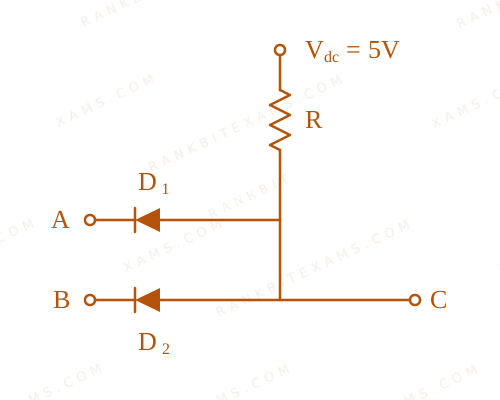
Q15 2025 Diode Rectifiers
In the circuit shown here, assuming threshold voltage of diode is negligibly small, then voltage mathrmV_AB is correctly represented by:
Diode Rectifiers diagram for Q15 - JEE Main 2025 Evening
An AC source connected across an orientation circuit involving an ideal junction diode.
  • A. mathrmV_ABtext would be zero at all times
  • B. {{IMG_OPT2}}
  • C. {{IMG_OPT3}}
  • D. {{IMG_OPT4}}

Solution

### Core Logic Analyze the cycle profile behavior of the input voltage waveform V = V_0 sin omega t: 1. **Positive Half Cycle**: Node A achieves a positive potential relative to node B. Under this configuration, the diode enters a **Reverse Biased (R.B.)** state, acting as an open switch circuit block. Since no current conducts across the resistive path, the potential difference tracked directly mirrors the input wave voltage. 2. **Negative Half Cycle**: Node A goes negative relative to node B. This transitions the diode into a **Forward Biased (F.B.)** condition, acting as a closed short-circuit bypass path. Consequently, the potential settles down immediately to zero. This behavior is visualized through the input/output tracking waveforms below:
Diode Rectifiers solution step diagram for Q15
An AC source connected across an orientation circuit involving an ideal junction diode.
Diode Rectifiers solution step diagram for Q15
An AC source connected across an orientation circuit involving an ideal junction diode.
### Step 1: Selection Matching this half-wave rectified configuration precisely selects option (4). ### Pattern Recognition When solving diode waveform problems, replace the diode mentally with an open circuit during reverse bias and a short circuit during forward bias to quickly observe the resulting output profile. ### Evaluation Rubric / Model Answer null ### Chapter Mix Class 12 Physics: Semiconductor Electronics
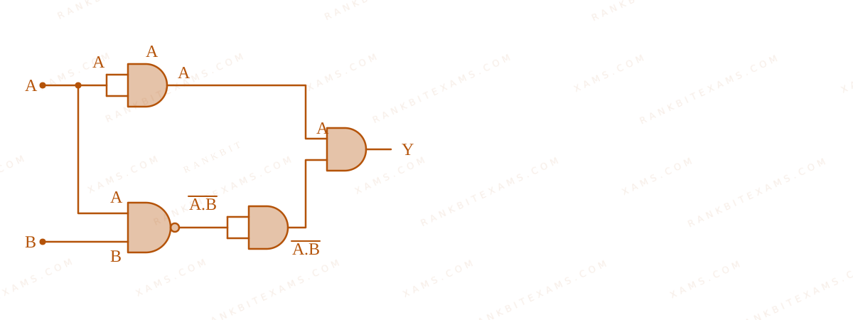
Q15 2025 Logic Gates
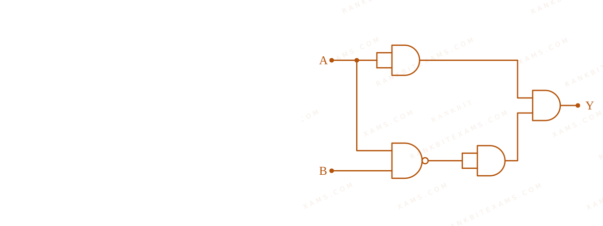
Logic Gates diagram for Q15 - JEE Main 2025 Morning
The image features a digital circuit blueprint constructed from basic logic gates with inputs A and B mapped to an output Y.
For the circuit shown above, equivalent GATE is : [cite: 1, 2]
  • A. OR gate
  • B. NOT gate
  • C. AND gate
  • D. NAND gate

Solution

### Core Logic Evaluating the given logic gate diagram combination step-by-step for all input permutations yields the following truth table :
Input AInput BOutput Y
000
011
101
111
This behavior matches an OR Gate configuration perfectly. ### Chapter Mix Class 12 Physics: Semiconductor Electronics
More Semiconductor Electronics Questions — jee_main_2025_04_april_evening

Practice all Semiconductor Electronics previous-year questions →

YOUR FIRST PREP STEP STARTS HERE

We Map Every Repeating Question in Competitive Exams.

Say goodbye to generic mock test fatigue. RankBit uses smart analysis to group past exam questions into their foundational Repeating Question Types. Find chapter weightage, track repeating questions, and score higher with targeted practice.

Select Your Target Exam

Choose an exam track below to find formulas per chapter and patterns.

Syncing Exam Intelligence

Mapping formulas and patterns across all tracks…

PATH A — FULL LENGTH PRACTICE

Full Mock Test Hub

Simulate real NTA exam conditions with fully tracked mocks. Time yourself against past papers.

Under Development
PATH B — TARGETED PRACTICE

Topic-wise Practice Hub

Practice past-year questions one chapter at a time. Pick an exam → subject → chapter and get every PYQ for that topic — pulled together from all past papers — with the chapter's key formulas alongside.

Loading Questions... Browse Topics
Latest from the Blog
View all →

Loading articles...